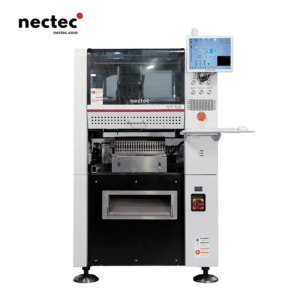

SIPLACE CA2 | Hybrid Mounter
As a hybrid combination of an SMT placement machine and a die bonder, the new SIPLACE CA2 can process both SMDs supplied from changeover tables and feeders as well as dies taken directly from the sawn wafer in a single work step. By integrating the complex die bonding process into the SMT line, it eliminates the need for special machines in production. With reduced personnel deployment, high connectivity, and integrative data utilization, the SIPLACE CA2 is therefore the perfect match for the Intelligent Factory.

SIPLACE CA2 | Hybrid Mounter
- Description
Description
1. Hybrid Placement System
Dual Process Integration
- Throughput: Achieves 50,000 die/hour (bonding) or 76,000 SMDs/hour (tape placement) with ±10μm @3σ accuracy, ideal for high-density advanced packaging (e.g., SiP system-in-package).
- Parallel Processing: A buffer storage module pre-fetches 16 new die during placement, enabling concurrent wafer picking and placement operations. For example, flip chip processing reaches 40,000 units/hour.
2. Wafer Handling & Feeding System
Wafer Management
- Rapid Wafer Changeover: Supports 50 unique wafer types with 6.5-second changeover time, minimizing downtime. Direct wafer feeding eliminates tape-out processes, saving up to 800km/year of tape waste and enhancing sustainability.
- Feeding Flexibility: Compatible with 8–56mm powered feeders, tube/tray components, and JEDEC trays. Optional wafer cassette or roll-to-roll trolley (COT) adapts to diverse production needs.
3. Vision Inspection & Metrology
High-Precision Recognition
- Laser Profiling: Real-time inspection of 0402 (01005 imperial) to 50×150mm odd-shaped components ensures placement accuracy.
- VCS Camera with Tricolor Illumination: Enhances fine-structure detection (e.g., BGA solder balls) with ±30μm accuracy via 3-color lighting technology.
- Die-Level Traceability: Provides bare die tracking from wafer slot to PCB position, meeting automotive electronics’ strict traceability requirements.
4. Motion Control & Automation
High-Speed Linear Drive System
- X/Y Axes: Utilizes high-precision linear motors with magnetic suspension and 0.001mm-resolution magnetic scales for optimized acceleration and stable placement.
- Dual Servo Y-Axis Drive: Reduces conveyor vibration and enhances long-substrate placement accuracy via optimized track transmission.
5. Software Ecosystem & Open Interfaces
Intelligent Software Suite
- JaNets Production Management: Enables offline programming (CAD import), placement path optimization, and simulation to reduce changeover time.
- WORKS Workshop Management: Integrates material loading verification and logistics optimization for improved OEE.
Open Automation Interfaces
- Supports IPC-CFX and SECS/GEM protocols for seamless MES/ERP integration, fulfilling smart factory data communication requirements.
specification
Placement speed | SMT up to 74,000 cph |
Die attach from Wafer up to 54,000 cph | |
Flip chip from Wafer up to 51,000 cph | |
Standard accuracy | 20μm 3 sigma |
Accuracy class | 15μm 3 sigma |
Accuracy class | 10μm 3 sigma |
PCB dimensions single lane conveyor (L x W): | up to 620 mm x 700 mm 20μm@ 3 sigma |
up to 620 mm x 700 mm 15μm @ 3 sigma | |
up to 620 mm x 700 mm 12μm @ 3 sigma(per 300 mm x 300 mm quadrant) | |
up to 300 mm x 300 mm 10μm @ 3 sigma | |
PCB dimensions dual lane conveyor (L x W): | up to 375mm x 260mm 20μm @ 3 sigma |
up to 375mm x 430mm 20μm @ 3 sigma (dual as single lane mode) | |
up to 250mm x 100 mm 15μm @ 3 sigma | |
up to 250 mm x 100 mm 10μm @ 3 sigma | |
Machine dimensions (L x W x H) | 2.56m * 2.50m * 1.85 m |


