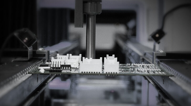
Printed Circuit Boards (PCBs) are the backbone of modern electronic devices, enabling complex circuit designs to be integrated into a compact space. As electronic components continue to evolve, understanding PCB loading becomes crucial for engineers and designers alike. In this post, we will delve into what PCB loading is, explore its importance, and discuss the best practices to optimize performance.
What is PCB Loading?
PCB loading refers to the way components are placed on a PCB and how their placement affects electrical performance. This includes factors like impedance, capacitance, and inductance, which can significantly impact a circuit’s efficiency and reliability. Different loading strategies are used to achieve desired electrical characteristics while minimizing issues like signal degradation or electromagnetic interference.
The Importance of PCB Loading
Effective PCB loading is essential for several reasons:
- Signal Integrity: Poor PCB loading can lead to signal loss and distortion, affecting the functionality of the device.
- Thermal Management: Components that are improperly loaded can generate excess heat, resulting in potential failure and reduced lifespan.
- Manufacturing Efficiency: A well-designed PCB layout can streamline manufacturing processes, reducing production costs and time.
- Compliance and Reliability: Adhering to PCB loading best practices can help in meeting industry standards and improving overall product reliability.
Key Factors Influencing PCB Loading
When designing PCBs, there are several key factors to consider that influence loading:
1. Component Type and Size
The type and size of components play a critical role in determining how they should be loaded on the PCB. Larger components may require more space and specific placement to maintain signal integrity, while smaller components can be densely packed.
2. Trace Width and Spacing
Trace width indirectly affects PCB loading since it influences current-carrying capacity and impedance. Designers must follow the appropriate standards to ensure that traces are wide enough to handle the necessary current while minimizing resistance.
3. Layer Stack-Up
The arrangement of layers in a multilayer PCB can significantly affect loading. A well-designed stack-up can enhance performance by controlling the return paths for signals and optimizing ground planes.
4. Ground and Power Distribution
Ground and power distribution should be carefully designed to minimize inductive coupling and ensure that signals return through the intended paths, preventing potential loading issues.
Best Practices for PCB Loading
Adhering to best practices is vital to achieving optimal PCB loading. Here are several strategies to consider:
1. Maintain Adequate Clearance
Ensure that there is enough clearance between components to prevent interference, particularly for high-frequency applications. This not only improves signal integrity but also facilitates easier assembly and repairs.
2. Optimize Component Placement
Strategically placing components can minimize trace lengths, thus reducing resistive and inductive losses. Group related components together and consider the flow of signals when designing the layout.
3. Use Ground Planes Wisely
Implementing a solid ground plane can reduce noise and interference. It provides a reference for signals, especially in high-speed circuits, and effectively manages return paths for current.
4. Employ Differential Pair Routing
When dealing with differential signals, routing pairs closely together helps maintain impedance and cancel out common-mode noise. This is particularly essential in high-speed digital designs.
5. Conduct Thermal Analysis
Perform thermal analysis during the design phase to identify hotspots and ensure that components are arranged in a manner that aids effective heat dissipation. Utilize thermal via and proper copper thickness to enhance cooling.
6. Simulate Before You Build
Utilize PCB simulation software to assess how your design behaves under various loading conditions. This can help identify potential issues early in the design process.
Common Mistakes to Avoid
Avoiding common pitfalls can help refine your PCB loading strategy:
1. Ignoring Layer Transitions
Make sure to properly manage transitions between layers to prevent abrupt changes in impedance, which can lead to signal reflection and loss.
2. Overlooking Component Specifications
Designers often neglect datasheets, which can lead to inappropriate loading conditions. Understanding voltage ratings, current limits, and thermal considerations is crucial for effective PCB designs.
3. Failing to Consider EMI/EMC Compliance
Electromagnetic Interference (EMI) and Electromagnetic Compatibility (EMC) should not be afterthoughts. Consideration for shielding and proper grounding techniques during the loading phase can mitigate interference issues down the line.
Future Trends in PCB Loading
As technology continues to advance, PCB loading will evolve as well. Below are some trends to watch:
1. Increased Integration of Components
With a push for miniaturization and increased functionality, engineers are likely to see more integrated components, which will alter traditional loading strategies.
2. Smart Manufacturing Techniques
The rise of smart manufacturing and automation will enable more efficient PCB loading processes, allowing for greater precision and fewer errors.
3. Advancements in Simulation Tools
Improved simulation software will allow designers to better predict how PCB loading will perform under a variety of conditions, leading to more robust designs.
Conclusion
As demand for compact, efficient electronic solutions continues to grow, mastering PCB loading becomes all the more essential. By following established best practices and avoiding common mistakes, engineers can significantly enhance the performance, reliability, and manufacturability of their PCBs.


