In the field of electronics manufacturing, semiconductor development boards serve as the core vehicle for hardware innovation, and their reliability directly determines the performance boundaries of end products. Through the deep integration of surface mount technology (SMT) and printed circuit board assembly (PCBA) processes, modern semiconductor development boards have achieved a leap forward in evolution from laboratory prototypes to industrial-grade products.
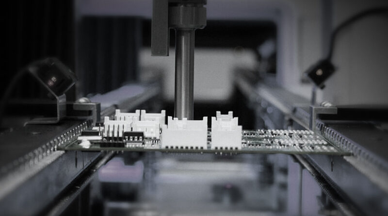
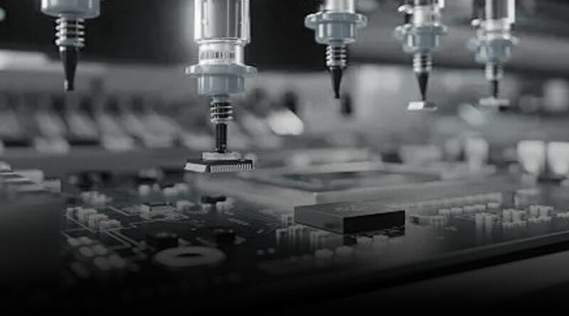
First, SMT is the cornerstone of precision manufacturing. SMT surface mount technology uses automated equipment to precisely mount micron-level components onto PCB substrates, and its technical advantages directly translate into improved reliability for development boards: High-precision assembly capabilities-modern SMT placement machines utilize optical alignment and in-flight inspection technology, achieving placement accuracy of ±0.05mm. They can reliably handle 0402-sized chips and high-density packaging components such as BGA and QFN. For example, in industrial IoT gateway development boards, SMT processes ensure millimeter-level placement accuracy for multi-protocol communication chips and RF modules, preventing signal interference; Welding quality optimization-the reflow soldering process precisely controls the temperature curve to form an ideal intermetallic compound layer with lead-free solder. Taking automotive electronics development boards as an example, they must pass a temperature cycle test from -40°C to 125°C. The SMT process optimizes pad design to extend the thermal fatigue life of solder joints to over 1,000 cycles; Production efficiency and consistency-automated production lines achieve placement speeds of tens of thousands of pieces per hour. Combined with AOI inspection equipment, defects such as cold solder joints and misalignment can be identified in real time. In the manufacturing of consumer electronics development boards, SMT production lines have increased the first-pass yield rate to over 99.5%.
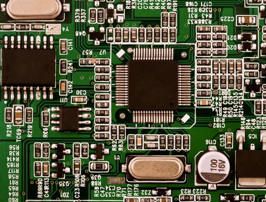
Second, PCBA processing guarantees the reliability assurance from design to mass production. PCBA manufacturing encompasses material selection, process control, testing, and verification, among other steps. Systematic management of these processes is critical to the reliability of development boards: Material compatibility design-the substrate uses high-Tg FR-4 boards to withstand the high temperatures of reflow soldering, and the solder uses a lead-free formula compliant with RoHS standards. In medical device development boards, AEC-Q200-certified MLCC capacitors are selected to ensure parameter drift remains below 5% in humid and hot environments; Process defect prevention-soldering process: nitrogen-protected reflow soldering reduces oxidation, and selective spraying technology is used in wave soldering to prevent bridging; Cleanliness control: plasma cleaning removes flux residues, and ion contamination is controlled to ≤1.5 μg/cm²; Stress Management: through the use of filling glue and reinforced rib design, the development board achieves vibration resistance performance of over 5G; Reliability testing system environmental testing: high-temperature aging and thermal shock testing verify thermal stability; Mechanical testing: random vibration testing simulates transportation impacts; Electrical testing: ICT online testing covers 100% of the circuit network.
Third, industry applications and their reliability-driven innovation scenarios. Industrial automation-in PLC development boards, SMT technology integrates multi-channel analog signal acquisition chips with isolated power supply modules. Through the application of three-proof paint and conformal coating technology, the boards can operate stably for over five years in the corrosive environment of chemical plants; Automotive electronics-the autonomous driving domain controller development board uses SMT-mounted 77GHz millimeter-wave radar chips. Through copper block heat dissipation design in PCBA processing, the chip junction temperature is reduced by 20°C, meeting the AEC-Q100 Grade-2 standard; Medical equipment-the portable ultrasound device development board integrates SMT-mounted ADC chips and low-noise LDOs. Through electromagnetic shielding design in PCBA processing, the image signal-to-noise ratio is improved by 15dB, meeting medical-grade EMC standards; Edge AI computing-in the AI inference development board, SMT technology enables 2.5D packaging of HBM memory and GPU chips. Combined with heat dissipation via-hole design in PCBA processing, this achieves a computing power density of 40 TOPS/W.
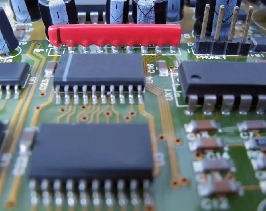
Fourth, the future direction of sexual technology evolution. There are some challenges ahead of this evolution for SMT industry. Micro-assembly technology: utilizing laser welding and flip chip technology to achieve reliable connections between components with a 0.3mm pitch; Smart detection: AOI equipment combined with AI vision technology can identify solder joint defects as small as 0.01mm in real time; Sustainable manufacturing: developing lead-free, halogen-free solder and biodegradable substrates to meet RoHS 3.0 requirements.
To conclude, the together innovation of SMT chip mounting technology and PCBA processing is reshaping the reliability boundaries of semiconductor development boards. From industrial parks to intelligent cars, from medical diagnosis to edge computing, highly reliable semiconductor development boards have become the foundation of digital transformation across various industries.


