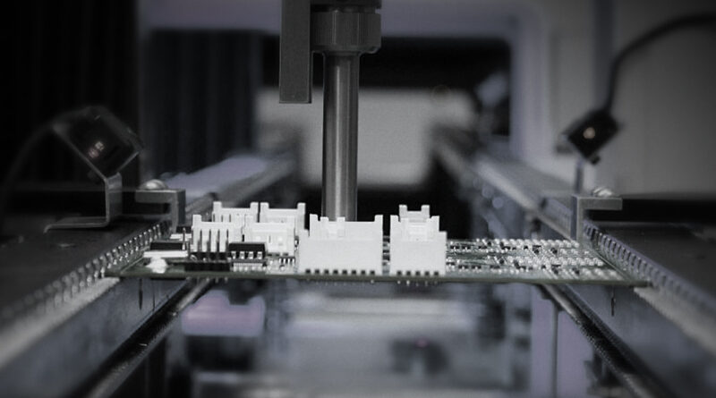
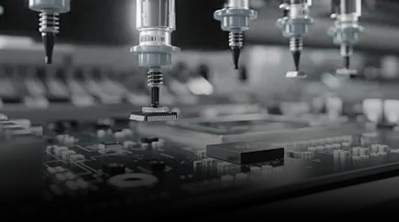
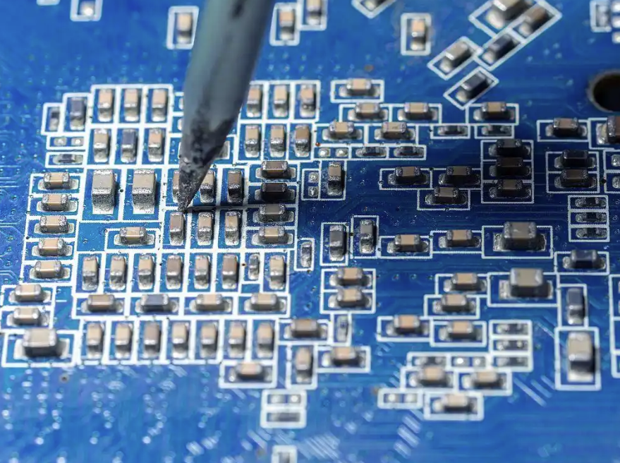
In the explosive growth of portable electronic devices, the Internet of Things terminal form continues to evolve, semiconductor development board as the core carrier of the electronic system is facing the triple challenge of “smaller size, higher integration, stronger performance”. As the core process of PCBA processing, SMT placement technology through the component miniaturization adaptation, high-density mounting process innovation and three-dimensional integration capability breakthroughs, to become the key engine to crack the development board miniaturization problems, to promote its consumer electronics, automotive electronics, aerospace and other fields to achieve the shape of the revolution. First, we would like to discuss about the physics behind the basis of the miniaturization of the electrical components. The core advantage of SMT placement technology is that it breaks through the size limitations of traditional through-hole insertion and provides a reliable physical carrier for ultra-miniature electronic components. Modern placement machines can accurately place 0201 (0.6mm x 0.3mm) or even 01005 (0.4mm x 0.2mm) sized chip components, with placement accuracy of ±50μm, to meet the alignment requirements of 0.3mm pin pitch QFP packages. Thanks to our Nectec’s pick and place machine series NT-P5, it is able to achieve flexible processing of the 0201 sized chip components using modular design support transformation technology. This capability enables semiconductor development boards to increase the density of component layout by 5-10 times: in smartphone baseband development boards, through the combination of 0402-size MLCC capacitors and 0.5mmpitch LGA packaged chips, the unit square centimeter can be integrated with more than 50 active and 200 passive components, which is more than 3 times the integration density compared to the traditional insertion process.
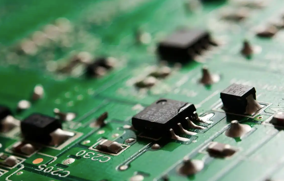
In the next topic, we will be discussing the real life application of this SMT technology advancement. There are three areas that we would like to focus on: consumer electronics, automobile electronics and aerospace industry. First to discuss about consumer electronics. In the smartwatch development board, the SMT process realizes the 0.4mm thickness of flexible PCB and 0.4mm height of ultra-thin components, such as our Nectec’s NT-L12 pick and place machine, with the curved surface mounting technology (mounting angle deviation <1°), so that the whole board can be bent with a radius of <5mm, which is perfectly adapted to the design of round watch cases. By controlling the height of components (the highest component ≤ 1.2mm), the overall thickness of the development board is compressed to less than 2.5mm, freeing up 30% of space for the battery and sensors. For automobile electronics, Automotive ADAS development board facing high temperature (-40 ℃ ~ +125 ℃), vibration (50g acceleration) of the harsh environment, SMT technology through miniaturization to achieve a compact layout: the use of 0.5mmpitch BGA package chip, with the bottom of the filling process (filling speed 50mm / s), in the 100mm × 100mm substrate integration of 6 AI chip with 20 Sensor interface, the volume is reduced by 60% compared with the traditional solution, and at the same time, the heat dissipation efficiency is improved through the optimization of component spacing (≥0.5mm).
For aerospace industry, Satellite payload development boards are sensitive to weight (cost per gram>$1000), SMT technology through lightweight material adaptation to achieve a breakthrough: the use of aluminum-based PCB (density 2.7g/cm³) instead of the traditional FR-4 substrate, with 0.1mm thickness of ultra-thin chip (weight <0.1g) mounting, so that the weight of the unit area to reduce the weight of 40%. Through the component layout optimization algorithm (genetic algorithm solution), 10 layers of circuit interconnections are realized on a 200mm×150mm substrate, which saves 20% space compared with manual layout.


