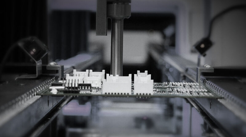
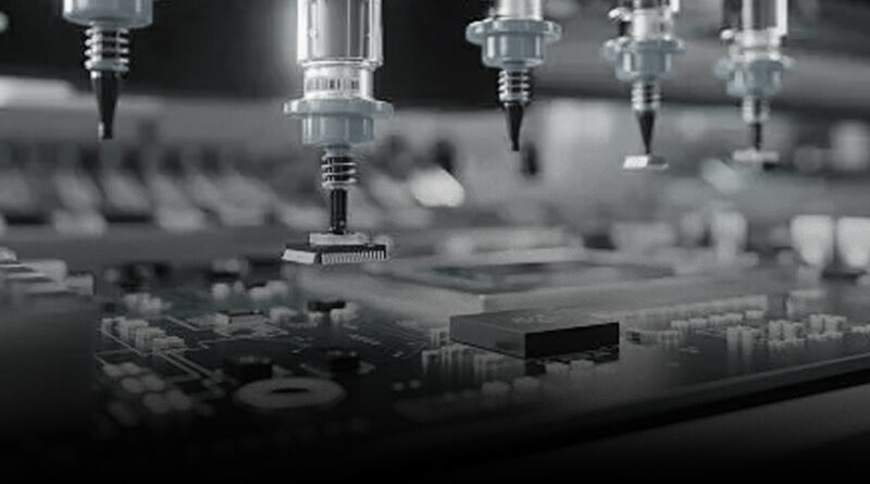
Sensors are one of the core components in Internet of Things (IoT) devices, and their performance directly affects the overall power consumption and battery life of the device. As IoT devices become smaller, smarter, and more energy efficient, optimizing the SMT assembly process in IoT PCBA manufacturing has become increasingly important. By optimizing the SMT assembly process, material selection, and design strategies, it is possible to effectively reduce sensor power consumption, extend device battery life, and improve overall energy efficiency.
First, let’s discuss the challenges pose on the reduction of the power consumption of IoT sensors. There are three main challenges that are worth mentioning. First challenge is high integration and complexity. IoT sensors typically integrate multiple functions, such as temperature, humidity, motion detection, etc., and their PCBA design must take into account signal processing, communication modules, and power management. High-density SMT mounting processes can increase circuit noise, which can affect sensor accuracy and power consumption; Second challenge is the limitation on the battery power supply. Most IoT devices rely on battery power, especially edge computing nodes and wireless sensor networks. Power consumption optimization directly affects device battery life and maintenance costs; Third challenge is the requirement for environmental adaptation. IoT sensors are often deployed in complex environments, such as industrial sites and outdoor settings, and must remain stable under extreme temperature or humidity conditions, which places higher demands on low-power design.
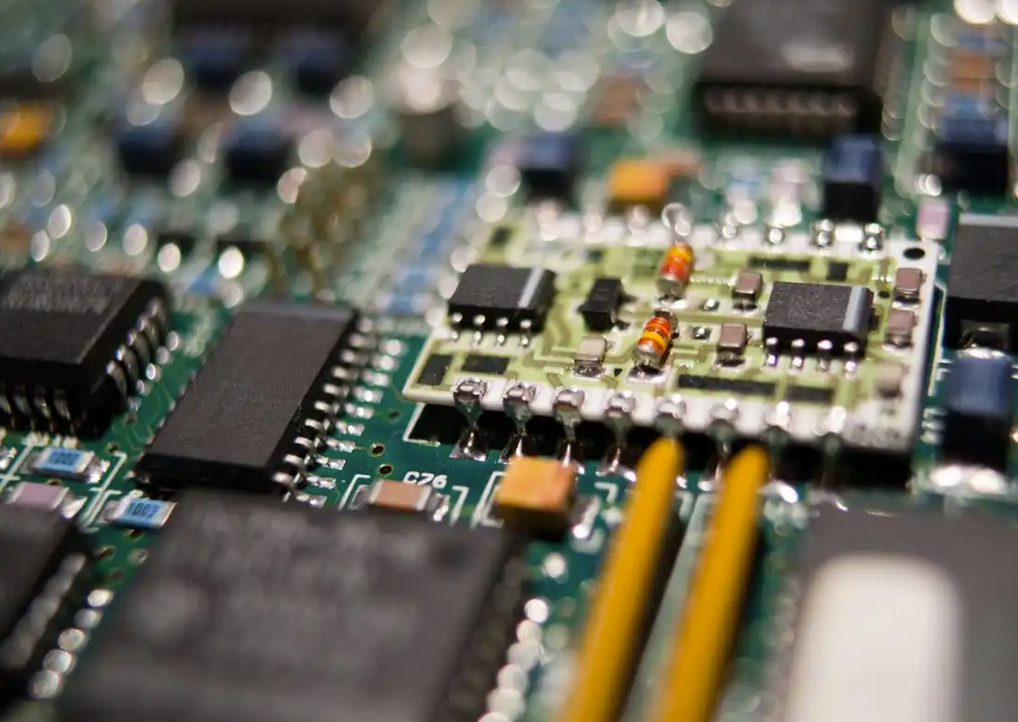
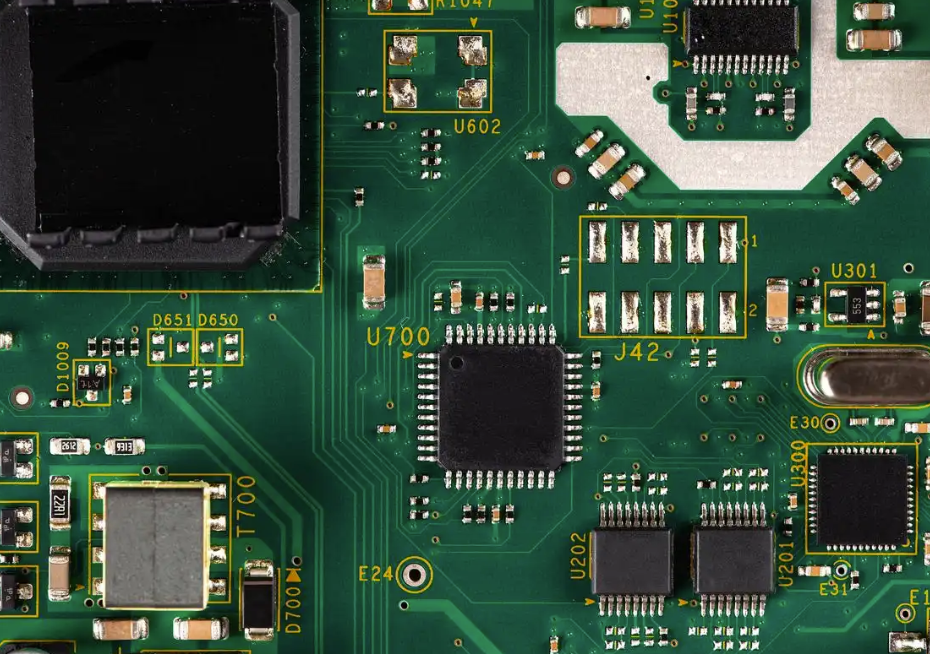
Second, let’s discuss the strategies for optimizing the power consumptions during the SMT manufacturing. There are five strategies that are worth mentioning. First strategy is choosing low-power components and packaging technology as a choice. The reason is because for low power consumption IC and sensor chips, low-power microcontrollers, sensor chips, such as MEMS sensors, and communication modules, such as LoRa and Bluetooth low energy, are preferred. For example, the ARM Cortex-M series MCU has a static current as low as 1μA, significantly reducing standby power consumption. Another reason is because for miniaturization packaging technology, SMT chip mounting technology supports ultra-small packages, such as 0402 and 0201 resistors and capacitors, reducing PCB area and wiring length, lowering parasitic inductance and resistance, and thereby reducing energy loss. On top, miniaturized packages can also reduce the thermal resistance of packaging materials and improve heat dissipation efficiency; Second strategy is optimizing PCB layout and routing. The reason is because for zone design and power isolation, it’s recommended to physically isolate high-power modules, such as RF communication modules, from low-power modules, such as sensor acquisition circuits, and supply them with power through independent power domains to avoid mutual interference. For example, in IoT sensor PCBs, design LDO regulators separately for sensor signal conditioning circuits to reduce dynamic power consumption. Another reason is because for differential signals and impedance matching, differential wiring design is usually used for high-frequency signal lines, such as I²C and SPI buses, to reduce electromagnetic interference and signal reflection, thereby reducing additional power consumption caused by repeated transmission.
At the same time, optimized impedance matching reduces energy loss during signal transmission; Third strategy is adopting intelligent power management solutions. The reason is because for dynamic voltage frequency control, it is more logically optimal to dynamically adjust voltage and frequency based on sensor workload. For example, when the sensor is idle, the MCU can automatically switch to a low-power mode, retaining power only to necessary peripherals. Another reason is because for energy gathering and storage design, they are often categorized as photovoltaics and piezoelectric materials. They can be combined with miniature supercapacitors to provide auxiliary power for sensors. For example, certain environmental monitoring devices use solar panels to power sensors, significantly reducing the consumption of the main battery; Fourth strategy is adopting precision control of SMT chip mounting process. The reason is because for solder paste printing and the optimization of reflow soldering, we can ensure that the solder joint quality and reduce additional power consumption caused by poor contact. For example, in IoT sensor PCBs, the use of nitrogen reflow soldering can improve solder joint reliability and reduce resistance loss during long-term operation. Another reason is because for automated inspection and defect prevention, using AOI and SPI technologies in the SMT assembly process enables real-time monitoring of solder joint quality, thereby preventing abnormal power consumption caused by cold solder joints or short circuits. For example, a smart home sensor reduced its soldering defect rate to 0.1% through AOI inspection, thereby reducing additional energy consumption caused by rework;
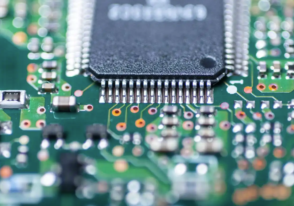
Fifth strategy is environmentally friendly design of materials and packaging. The reason is because for low dielectric constant substrate, it helps to reduce medium loss in high-frequency signal transmission, and so reducing power consumption as well. Another reason is because for thermal conductive materials and heat dissipation design, we can add thermal silicone or metal shielding around the sensor module to reduce additional power consumption caused by chip temperature increases through efficient heat dissipation.
Third, let’s discuss some future prospect toward the development of SMT technology and IoT devices. First, AI-driven SMT process optimization can use complex algorithms to analyze SMT placement data such as solder joint quality and temperature curves. And then adjust process parameters in real time to minimize power consumption. For example, machine learning is used to predict the probability of solder joint defects and optimize the reflow soldering temperature curve in advance; Second, flexible PCBs, irregularly shaped packaging and IoT sensor PCBA processing can potentially adopt flexible substrates and irregularly shaped packaging, further reducing material waste and power consumption. For example, flexible PCBs can reduce wiring length and lower signal transmission loss; Third, Energy-self-sufficient IoT devices, combined with SMT-mounted micro energy harvesting modules can achieve “zero power consumption” operation, completely solving the problem of battery replacement.

To conclude, the low-power design of IoT sensors relies heavily on the refined optimization of SMT assembly processes. By selecting low-power components, optimizing PCB layout, implementing intelligent power management solutions, and enhancing SMT assembly quality, it is possible to significantly reduce device power consumption, extend battery life, and meet reliability requirements in complex environments. With advancements in material innovation and smart manufacturing technologies, the energy efficiency of IoT sensors will continue to improve, providing a solid foundation for sustainable development in fields such as smart cities, industrial internet, and healthcare.


