With the increasing demand for miniaturization, high integration, and high efficiency in smart home lighting systems, SMT assembly technology has become a core component in LED lighting manufacturing. However, the luminous efficiency and heat dissipation performance of LEDs directly determine the brightness, lifespan, and stability of lighting fixtures. We will explore how to ensure high luminous efficiency and effective heat dissipation through technical means by examining three aspects: the smart home PCBA manufacturing process, SMT assembly process optimization, and heat dissipation design strategies.
First of all, let’s discuss some key stages for smart home PCBA processing. Stage 1-PCB design and material selection. In the PCB design of smart home lighting devices, heat dissipation performance should be a top priority. For example, metal substrates (such as aluminum substrates) can be used to replace traditional FR-4 substrates, as they have a higher thermal conductivity, such as the fact that aluminum sub-station boards can reach 1-3 W/m·K. Which enables rapid conduction of heat generated by LEDs to the heat dissipation layer. Also, multi-layer PCB designs can increase heat dissipation pathways by optimizing the distribution of copper foil in inner layers to improve heat conduction paths and reduce localized high-temperature areas; Stage 2-precise control of SMT chip mounting process. Steel mesh printing and solder paste quality are important because laser steel mesh precisely controls solder paste thickness for 80-150μm typically to ensure solder joint uniformity, avoiding false soldering or short circuits caused by insufficient or excessive solder paste, thereby reducing local thermal resistance.
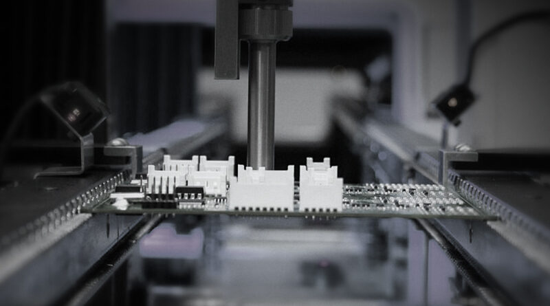
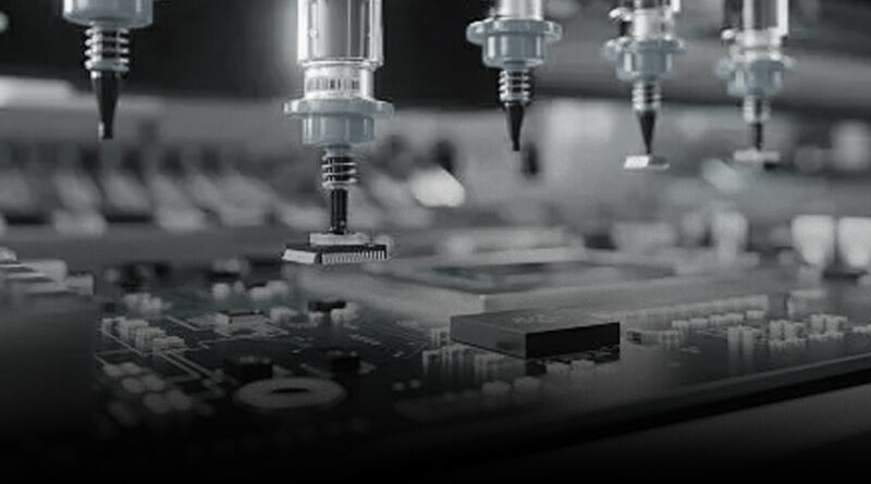
SMT placement accuracy and AOI inspection are necessary because the SMT placement machine uses vacuum nozzles, like Nectec’s NT-B5 utilizing ATC automatic nozzle system and real time vacuum detection, and image recognition systems (such as mark point calibration) to ensure the precise placement of LED chips, avoiding uneven heat dissipation caused by misalignment. Online AOI inspection can detect soldering defects in real time, improving yield rates. Reflow soldering temperature curve are also necessary because they set a reasonable temperature curve, stages are preheating, constant temperature, reflow, and cooling, to ensure that the solder paste melts completely without damaging the LED chip. For example, control the peak temperature between 230-250°C to avoid high temperatures causing the LED packaging material to age.
Second of all, let’s discuss key points for describing the core strategies for LED heat dissipation design. Key point one-applications of highly efficient heat-conducting materials. Thermal interface materials are used to fill the space between the LED chip and the heat sink substrate with thermal grease or thermal pads to reduce contact thermal resistance and improve heat transfer efficiency. Heat sink and fin structure are categorized as the design aluminum heat sinks or fin structures for smart lighting fixtures to accelerate air convection heat dissipation by increasing the surface area. For example, forced air cooling heat sinks can reduce junction temperature by 5-10°C, significantly extending LED life; Key point two-combination of active and passive cooling.
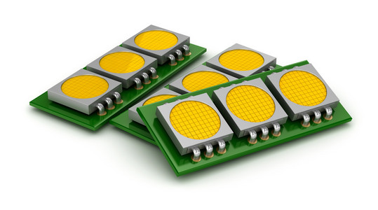
Peltier technology is defined as some high-power LED luminaires use thermoelectric cooling modules, such as the TEC1-12706 model we are all familiar with, to absorb heat at the cold end and dissipate heat at the hot end with a fan, achieving rapid temperature control, which is particularly suitable for enclosed smart luminaires. Intelligent temperature control system actively and cohesively integrates temperature sensors, such as NTC thermistors we know, monitor the LED junction temperature in real time and dynamically adjust the drive current through the MCU to prevent light decay caused by overheating. For example, when the temperature exceeds 65°C, the brightness is automatically reduced by 10%-20% to balance light efficiency and heat load; Key point three-environmental optimization and structural design. Ventilation layout optimization is used to design heat dissipation holes or air ducts in the luminaire housing to enhance heat dissipation through natural convection. Avoid thermal resistance accumulation depicts the phenomenon of reducing thermal resistance interference between multiple layers of material.
Third of all, let’s discuss some special requirements for SMT manufacturing techniques in the use of smart home devices. Requirement one-miniaturization and high-density mounting. Smart home lighting fixtures are becoming more compact, requiring the use of miniature LEDs in 0201 or 0402 packages, which places higher demands on the precision of SMT placement machines, usually ≤ 0.05 mm. At the same time, component layout should be optimized to avoid heat concentration, such as evenly distributing high-power LEDs across the PCB; Requirement two-moisture protection and reliability assurance. Interestingly, we suggest that before SMT processing, bake the PCB at around 120°C for at least 2 hours to remove moisture and prevent bubbles from forming during reflow soldering, which could cause soldering failure.
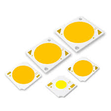
Not only this, it’s recommended to use high-temperature resistant packaging materials, such as silicone rubber instead of epoxy resin to reduce long-term light decay. Experiments show that silicone rubber-packaged LEDs can extend their service life to 40,000 hours under the same temperature conditions.
Fourth of all, let’s discuss a case study for heat dissipation solution for smart dimmable lighting fixtures. In one of our past customers’ projects for smart ceiling lighting fixtures, his engineers first designed the aluminum substrate and copper foil heat dissipation layer combined with bottom heat dissipation fan. Then, his factory conducted SMT placement using high-precision general-purpose machines to ensure uniform distribution of LED arrays. Lastly, they integrated with a Bluetooth module and temperature control chip, users can adjust brightness and view real-time temperature via the app. What made him thrilled is that the test results show that when operating at full load, the lamp’s junction temperature remains stable below 55°C, with a light output maintenance rate exceeding 90% and a lifespan of 50,000 hours.
In the end, the future for the smart lighting fixtures SMT technology is bright. With the utilization of innovative materials. Not only graphene thermal film with a thermal conductivity of 5300 W/m·K and aluminum nitride ceramic substrate with a thermal conductivity of 170 W/m·K will further improve heat dissipation efficiency, but also combining AI algorithms to predict heat distribution, dynamically adjust cooling strategies, such as automatically switching between active and passive cooling modes based on ambient temperature.
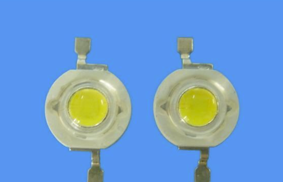
It is utterly crucial for SMT factories to realize that by optimizing the PCBA manufacturing process, innovating heat dissipation design, and implementing strict process control, smart home lighting systems can achieve efficient heat dissipation while maintaining high luminous efficacy, thereby meeting users’ comprehensive requirements for brightness, lifespan, and smart control.


