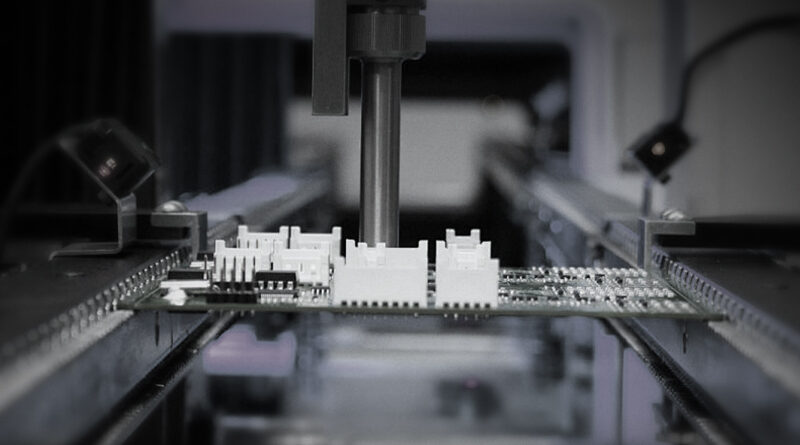
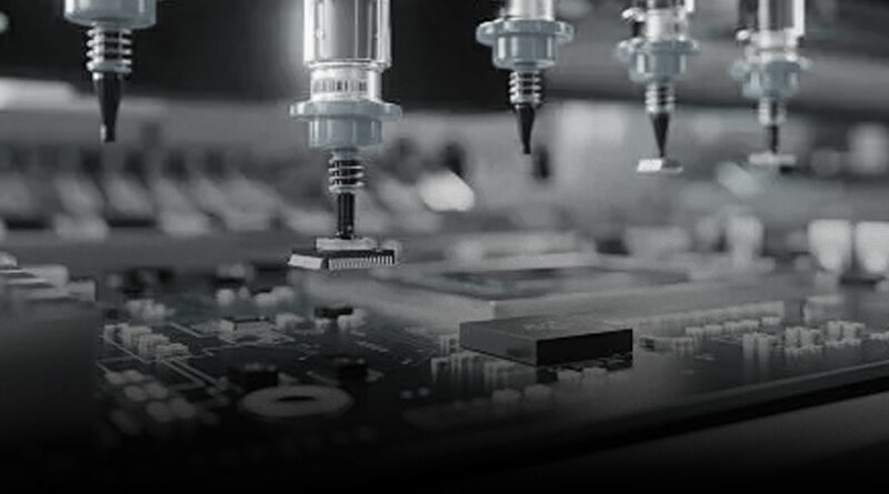
How do electrical components smaller than a grain of rice on a cell phone’s motherboard “stick” to the PCB and conduct electricity? The answer lies in the soldering process of Surface Mount Technology (SMT). SMT technology has been involved in the cellphone chips industry for a long time. Here is the detailed steps for soldering electrical components onto the PCB using the newest SMT technology. Step one, Finding a good “landing spot” for components. The first step in surface mount soldering is to apply an appropriate amount of solder paste to the pads of the PCB – a mixture of solder powder (20-50 μm in diameter), flux and adhesive that looks like gray “toothpaste”. Our Nectec’s solder paste printer series-SP-510A can handle such tasks. It supports boards up to 510mm x 510mm and is suitable for electronics, automobile and telecommunications. Now, the second step is to mount the electrical components on the correct spot led by the vision automated machine. The PCB coated with solder paste is fed into the mounter, which is like a “precision robot” that can complete the placement of a dozen components in one second. Our Nectec’s pick and place machine series NT-T5 matches the description, with an impressive placement speed of 84,000 CPH and placement accuracy of ±0.035mm (XYZ). The “eye” of the mounter is a high-definition camera, which calculates the exact position by identifying the datum point on the PCB and the shape of the component, and then sucks up the component with a vacuum nozzle (minimum diameter of 0.3mm) and puts it in the center of the pad.
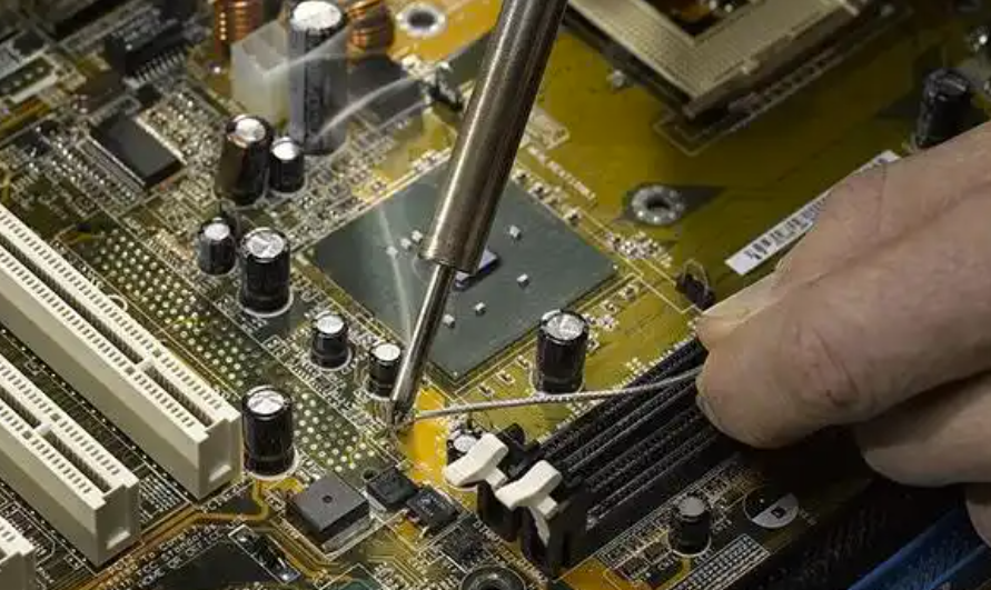
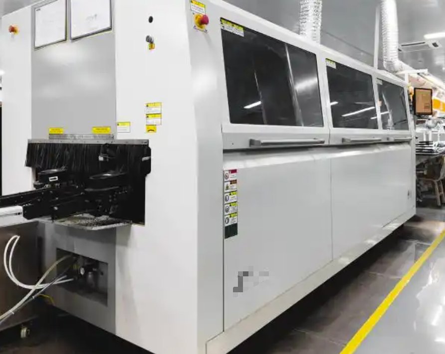
There are two mainstream welding processes: from “localized heating” to “total reflow”. For total reflow soldering, it simply means letting solder paste “flow itself into a solder joint”. The PCB with components attached enters the reflow oven, where the solder paste is heated through four temperature zones to complete the transition from “paste” to “solder joint”: Preheating zone (80-150°C): evaporates water and solvents in the solder paste, activates the flux, and removes the oxidized layer, taking about 60-90 seconds. Constant Temperature Zone (150-180°C): Further heating without melting the solder, preventing damage to components due to sudden heat, 30-60 seconds. Reflow zone (220-250 ° C): solder powder melting (melting point of solder about 183 ° C), liquid solder in the surface tension automatically fill the gap between the pad and the component pins, the formation of smooth solder joints, the highest temperature needs to be more than the melting point of 30-50 ° C, but the residence time should not exceed 10 seconds, otherwise it will be burned components. Cooling zone: the solder joint quickly cooled and solidified (cooling rate of 5-10 ℃ / sec), the formation of a solid metal connection. Our Nectec’s lead free reflow oven series contain a comprehensive product line. From the minimum 4-5 zones to maximum of 12 zones reflow oven that supports up to 300mm of PCB width. For 8, 10 and 12 zones of reflow ovens, what’s special about these three products is that they all support one-rail, dual-rail nitrogen soldering, providing comprehensive functions to ensure the success of soldering.
