In the era of renewable energy, the importance of inverters cannot be overstated. They serve as vital components in converting DC power to AC power in various applications, including solar energy systems, electric vehicles, and grid power supply. This article delves into the intricate world of PCB (Printed Circuit Board) assembly for inverters, outlining essential components, assembly processes, and key considerations for optimal performance.
What is PCB Assembly and Its Role in Inverters?
PCB assembly is the process of assembling electronic components onto a printed circuit board to create functional electronic devices. Inverters rely on PCBs to manage power conversion processes effectively. A well-assembled PCB ensures reliability, efficiency, and longevity of the inverter.
Key Components of Inverter PCBs
Understanding the PCB assembly process begins with familiarizing yourself with the key components typically found in inverter PCBs:
- Transistors and MOSFETs: These components are fundamental for switching actions in the inverter, allowing for the efficient modulation of power.
- Capacitors: Used for filtering and energy storage, capacitors help smooth out voltage fluctuations and ensure stability in performance.
- Inductors: Integral to controlling the flow of current, inductors also play a role in smoothing the output voltage.
- Microcontrollers: These act as the brain of the inverter, managing the various operations and ensuring efficient energy conversion.
- Diodes: Often used for protection and rectification within inverter circuits, diodes help maintain optimal performance.
The PCB Assembly Process
The process of PCB assembly can be broken down into several stages, ensuring that all components are integrated correctly and efficiently.
1. Design and Layout
The first step involves designing the PCB layout using specialized software. This stage includes choosing the right materials, specifying the dimensions of the board, and determining the placement of components based on electrical considerations.
2. Schematic Capture
Once the layout is designed, engineers create a schematic diagram that serves as a blueprint for the assembly process. This diagram outlines how each component will be connected to one another, ensuring a seamless flow of electricity.
3. Component Placement
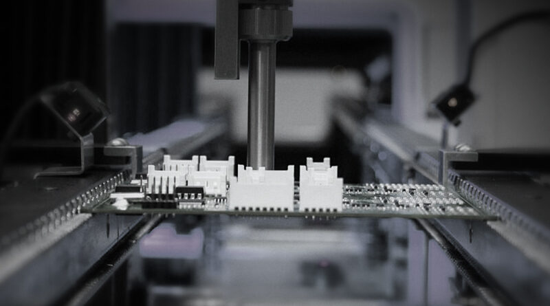
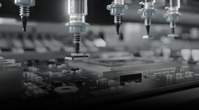
After the design is finalized, components are placed on the PCB. Automated machines often perform this task, ensuring precision and speed. However, manual assembly may be required for complex components or small batches.
4. Soldering
Next comes soldering, which involves joining the components to the PCB using solder. There are several soldering techniques, including:
- Wave Soldering: Useful for through-hole components, wave soldering passes the entire PCB over a wave of molten solder.
- Reflow Soldering: Primarily for surface-mount components, this method heats the solder paste that melts to connect the components.
5. Inspection and Testing
Post-assembly, the board undergoes thorough inspection and testing. Automated Optical Inspection (AOI) systems are often employed to detect soldering defects, misplacements, or component failures. Functional testing ensures that the inverter operates correctly under expected conditions.
Key Considerations for High-Quality PCB Assembly
To achieve optimum performance and reliability of inverters, several factors must be taken into consideration during the PCB assembly process:
1. Material Choice
The materials used for the PCB significantly impact its durability and performance. FR-4 fiberglass is common for general applications, but thermal management can be improved using materials like aluminum or polyimide for high-power applications.
2. Thermal Management
Inverters generate substantial heat, making thermal management critical. Effective cooling solutions—like heatsinks or fans—must be integrated into the design to prevent overheating and ensure optimal functionality.
3. Size and Form Factor
Depending on the application, the size and form factor of the PCB can vary. Designing compact PCBs without compromising the integrity of the components can lead to enhanced performance and efficiency.
4. Compliance with Standards
Ensuring that the PCB assembly complies with industry standards—such as IPC-A-610 for acceptability of electronic assemblies—is essential for quality assurance and reliability.
The Future of PCB Assembly in Inverters
The field of PCB assembly for inverters is continually evolving, embracing advances in technology and materials. Here are a few trends to watch out for:
1. Automation and AI Integration
As automation technology matures, more PCB assembly processes will rely on AI and robotics, leading to increased efficiency and reduced human error.
2. Thinner and Flexible PCBs
As demand for compact electronic devices grows, the shift towards thinner and more flexible PCBs will become increasingly prevalent, allowing manufacturers to integrate higher functionality into smaller spaces.
3. Focus on Sustainable Practices
The importance of sustainability is rising in every sector, including electronics manufacturing. The use of eco-friendly materials and processes will become more critically evaluated as the market evolves.
Conclusion
Understanding the intricacies of PCB assembly for inverters is essential for manufacturers aiming to deliver high-performance products. From the components used to the processes followed, each aspect plays a pivotal role in the overall success of inverter applications across various industries.


