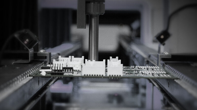
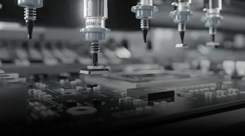
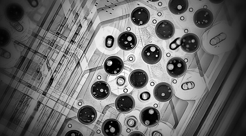
In this passage we will discuss the principles of X-ray inspection technology. The core of X-ray inspection technology lies in utilizing the penetrating properties of X-rays to visualize the internal structure of objects. When X-rays pass through materials of different densities, they are absorbed to varying degrees due to these density differences, thereby forming corresponding internal images. Specifically, denser metallic materials, such as solder joints, exhibit strong absorption of X-rays, resulting in distinct contour images. In contrast, materials with lower density, such as PCB substrates or voids within solder joints, absorb fewer X-rays, leading to varying gray-scale levels in the images. After the inspection equipment accurately captures these differences, it can construct precise images of the object’s internal structure, providing intuitive evidence for subsequent defect detection and analysis. In SMT assembly, the solder balls of packaging types such as BGA (ball grid array) and CSP (chip-scale packaging) are located at the bottom of the pins, and the solder joints are covered by the packaging body, making it difficult for traditional optical inspection (AOI) to effectively check their soldering quality. We will explain some of the applications that X-ray machines can be useful in inspecting the defects of SMT products.
First application is soldering joint void detection. During the reflow soldering process, if the gas in the solder paste cannot be completely removed, it will form voids in the solder joints. The presence of these voids weakens the structural strength of the solder joints, reduces their electrical conductivity, and may even cause premature failure of electronic components.

Second application is bridge problem detection. During the soldering process, excessive solder or inaccurate solder pad placement may cause bridging between solder joints. Bridging
can disrupt the normal electrical performance of the circuit and cause faults such as short circuits. X-ray inspection can clearly show the solder distribution between solder joints
and accurately detect whether there are any excess solder bridges to ensure that the electrical performance of the circuit meets design requirements and promptly eliminate this
safety hazard.
Third application is open circuit and cold solder joint detection. In some cases, due to incomplete solder melting or improper welding operations, cold solder joints or open circuits may occur. These welding problems can seriously affect the electrical conductivity of the circuit, causing electronic devices to malfunction. X-ray inspection can easily identify a series of welding defects such as cold solder joints and open circuits by carefully inspecting the density and shape of the solder joints, providing accurate evidence for timely repairs and ensuring the performance and quality of electronic products.
Now, we will discuss some advantages of such X-ray machines inspection technology. First advantage is lossless testing characteristics. X-ray inspection is a non-destructive testing method that does not cause any physical damage to PCBs or welded parts. This feature allows
manufacturers to monitor welding quality in real time during the production process, promptly identify and resolve potential issues, without worrying about adversely affecting the performance of the final product. Compared to some destructive testing methods, X-ray inspection can ensure product quality while reducing testing costs and improving production efficiency.
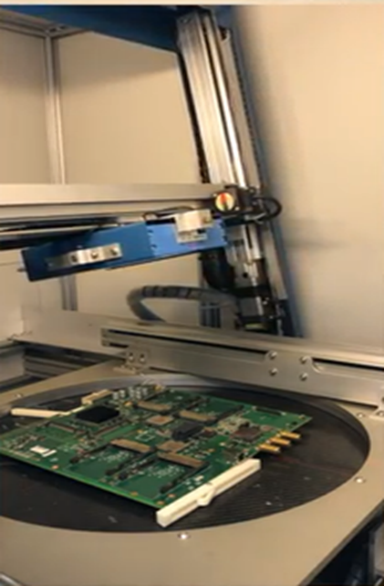
Second advantage is high-resolution imaging and high reliability. X-ray inspection technology can perform high-resolution imaging of small details such as solder joints, ensuring comprehensive and detailed inspection of welding quality. Even internal defects that are difficult to detect using traditional inspection methods can be clearly revealed through X-ray images, providing inspectors with accurate and reliable inspection results. This highly reliable inspection method helps improve the overall quality of products and enhance market competitiveness.
Third advantage is the ability to handle complex packaging structures. With the development of the electronics industry, high-density, complex PCB packaging structures such as BGA, CSP, and PoP are becoming increasingly common. The soldering quality of these packaging forms is critical to the overall performance of the circuit board, yet traditional inspection methods often struggle to address these challenges. X-ray inspection technology, with its powerful penetration capability and precise imaging effects, can easily meet the inspection requirements of these complex packaging structures, promptly identify and repair potential soldering defects, and ensure the high-performance operation of the circuit board.
Fourth advantage is the ability to support batch testing and automated production. X-ray inspection technology can be used not only for individual PCB inspection, but also for online inspection in mass production processes. Combined with advanced automation equipment, X-ray inspection enables fast and efficient quality control in large-scale production processes.
This not only improves production efficiency, but also ensures that the soldering quality of each PCB meets strict standards, providing a strong guarantee for the stable production of electronic products.
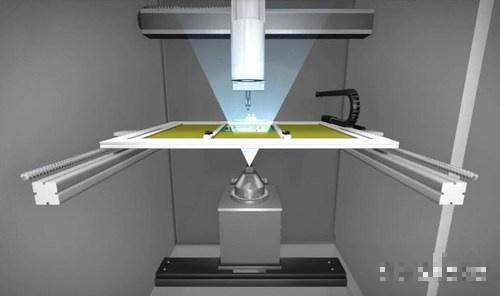
Now, we will discuss some of the common problems and the corresponding solutions to these X-ray inspection machines. First problem can be void soldering joints problem. Voids inside solder joints are one of the most common defects in SMT assembly, especially during BGA soldering. Excessively large voids can weaken the mechanical strength and electrical conductivity of solder joints, affecting the stable operation of electronic components. X-ray inspection technology can accurately measure the size, shape, and distribution of voids, ensuring that the void rate is controlled within a reasonable range.
Second problem can be soldering ball deformation or depression issues. During BGA soldering, deformation or indentation of solder balls can seriously affect the soldering results. Abnormal solder ball shapes can lead to poor contact at solder joints, reduced electrical conductivity, and even false soldering. X-ray inspection can clearly detect abnormal solder ball shapes and provide early warning of soldering quality issues.
Third problem can be workpiece misalignment issues. During the SMT assembly process, machine malfunctions, operator errors, or material quality issues may cause workpieces to become misaligned. Workpiece misalignment affects the installation accuracy and electrical performance of electronic components, which in turn leads to product malfunction. X-ray inspection can check the accurate position of workpieces, promptly detect and correct misalignment issues.
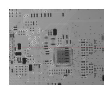
To conclude, in modern electronics manufacturing, electronic components and circuit boards are becoming smaller and smaller, and their functions are becoming increasingly complex, which places higher demands on SMT chip processing inspection technology. X-ray inspection technology, with its efficient, lossless, and accurate inspection advantages, has become an effective means of addressing soldering defects that are difficult to detect using traditional optical inspection methods. It not only ensures the reliability of high-density circuit board soldering, but also significantly improves the overall quality control level of the production process.


