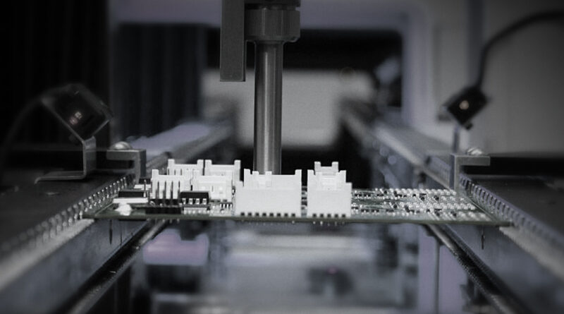
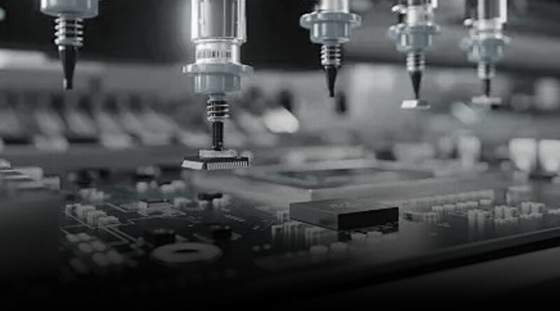
In the process of semiconductor technology continues to break through the physical limit, SMT (surface mount technology) as the core process of PCBA processing, and semiconductor development boards are forming a deep technical symbiosis. This synergy not only reshapes the underlying logic of electronics manufacturing, but also promotes development boards to realize leapfrog improvement in key indicators such as integration density, signal integrity and reliability. First, let’s discuss technology symbiosis. The miniaturization of semiconductor components and functional integration directly promote the evolution of the SMT process to higher precision. BGA (Ball Grid Array) package, for example, when the pin spacing from 0.5mm narrowed to 0.3mm, the visual positioning accuracy of the SMT placement machine needs to be improved from ± 50μm to ± 15μm, while with our Nectec’s pick and place machine series NT-B5 to achieve a high degree of consistency of the control of the solder ball. This process breakthrough enables semiconductor development boards to integrate 1000+ pin SoC chips to support the realization of complex systems such as 5G base station RF modules. On the other hand, process innovation in SMT feeds semiconductor design freedom. The application of nano-silver conductive pastes boosts solder joint thermal conductivity to 80W/m・K, a 50% improvement over traditional solder pastes, reducing junction temperatures of power semiconductor devices by 15°C at full load, thus allowing chip design to relax power consumption constraints. This material breakthrough provides a thermal solution for high-performance development boards such as AI gas pedals and automotive power modules. Secondly, let’s discuss performance reconstruction. SMT mounting technology breaks through the physical limit through the ability of ultra-miniature component mounting.
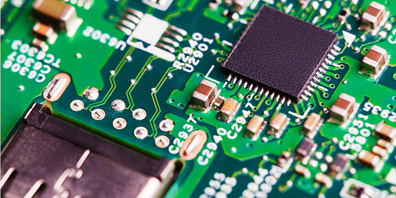
01005 components (0.4mm x 0.2mm) stable mounting enables the development board to increase the number of components per unit area by 5 times, which supports the integrated design of multi-chip modules (MCM). In medical device development boards, this capability realizes the integration of a 128-channel bioelectric signal acquisition module in a 10mm x 10mm size, which is 80% smaller than conventional plug-in solutions. On the other hand, SMT’s short-pin design significantly reduces parasitic parameters in high-frequency, high-speed scenarios. Taking 5G millimeter wave development boards as an example, SMT patch reduces the signal path parasitic inductance from 5nH in through-hole technology to less than 0.1nH, which, together with the LCP (liquid crystal polymer) substrate (dielectric constant of 2.8, loss factor of 0.002), can support stable transmission of signals above 60GHz with a BER of less than 10^-12. This performance enhancement directly promotes technological breakthroughs in the areas of vehicle-mounted radar and satellite communications. This performance improvement directly promotes the technological breakthrough in the field of vehicle radar, satellite communication, etc. Thus, to build such reliable foundation like this, SMT responds to complex working conditions through multi-dimensional process optimization. In the industrial control development board, Sn96.5Ag3.0Cu0.5 alloy solder paste combined with stepped pad design, so that the tensile strength of the solder joints ≥ 0.15N/mm ², compared with the traditional design to improve 25%; at the same time, injected into the bottom of the filler to absorb 90% of the vibration energy, to ensure that the fatigue life of the joints in the -40 ℃ to 125 ℃ temperature cycle of more than 10 ^ 6 times.
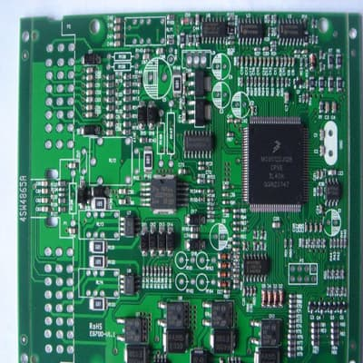
Third, let’s discuss about the real life application of SMT technology. First is the traditional electronics field. The smartphone motherboard realizes component density up to 25 per square centimeter through SMT, and supports the integration of 5G RF module and AI chip. Wearable device development boards using flexible circuit boards (FPC) as a carrier, using low-temperature curing adhesive (curing temperature <150°C) to complete the 3D stacking package of sensors and batteries, and maintaining signal transmission stability under the condition of bending radius <2mm. Second is the electrical automobile field. In-vehicle ADAS development boards realize the mass production of 0.3mm pitch BGA devices through SMT, and control the defect rate of solder joints to less than 5 parts per million with X-ray inspection system. In the battery management system for new energy vehicles, the copper-based heat dissipation pads and micro-channel design of the SMT patches reduce the module thermal resistance to 0.5K/W and meet the IP67 waterproof and dustproof requirements. Last is the industrial automation field. The PLC development board uses SMT nano-silver conductive paste to realize highly reliable interconnections, and signal transmission delay fluctuations <5ps under vibration acceleration ≥5 g. This process breakthrough enables the industrial robot controller to improve response speed by 30%, while supporting -20℃ to 85℃ wide temperature range operation. At the end of this passage, we would like to mention the prospect of this SMT technology advancement.
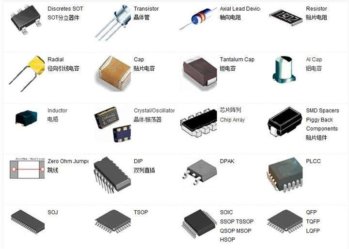
First, we are looking at complete digitized transformation. The AI-driven AOI inspection system realizes micron-level defect recognition through deep learning, with a misjudgment rate of less than 0.1%, and provides real-time feedback to adjust placement parameters-our Nectec’s NX-B uses two power x ray penetration inspection object technology to accurately detect the interior defects. The application of digital twin technology has shortened the new product introduction cycle by 30% and increased the accuracy of equipment failure prediction to 95%. Second, we are looking at building a foundation for the new material. Phase change energy storage solder dynamically adjusts heat distribution during the soldering process, reducing the thermal shock of high-power device soldering by 40%; the application of degradable PI film promotes the evolution of medical implantable development boards towards environmental protection, and realizes the balance between biocompatibility and signal stability in the in vivo environment.


