Gedruckte Schaltungen (PCBs) sind das Rückgrat der Elektronik und dienen als Hauptverbinder für elektronische Komponenten. Bei der Herstellung dieser komplexen elektronischen Geräte ist die Qualitätskontrolle von entscheidender Bedeutung. Eine der wichtigsten Technologien zur Gewährleistung der Zuverlässigkeit und Qualität von Leiterplatten ist die Röntgenprüfung. Dieser Artikel befasst sich mit der Bedeutung der Röntgenprüfung von Leiterplatten, ihren Vorteilen, Methoden und ihrer zunehmenden Bedeutung für die Zukunft der Elektronikfertigung.
Verständnis der PCB-Röntgeninspektion
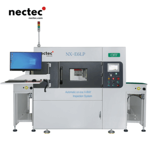
Bei der Röntgenprüfung von Leiterplatten wird elektromagnetische Hochfrequenzstrahlung eingesetzt, um die innere Struktur von Leiterplatten sichtbar zu machen. Diese zerstörungsfreie Prüftechnik ermöglicht es den Herstellern, die Zusammensetzung der Leiterplatte zu analysieren, ohne sie zu beschädigen.
Mit dieser Methode lassen sich Defekte oder Probleme wie Lötstellen, Risse, Fehlausrichtungen und versteckte Verbindungen schnell erkennen. Durch den Einsatz der Röntgentechnologie können Hersteller die Integrität der Lötstellen, die die Komponenten mit der Platine verbinden, sicherstellen, was für die Zuverlässigkeit der Geräte entscheidend ist.
Warum ist die Röntgeninspektion bei der Leiterplattenherstellung so wichtig?
Die zunehmende Komplexität von Leiterplatten erfordert sorgfältige Prüfverfahren. Im Folgenden werden einige Hauptgründe genannt, warum die Röntgenprüfung von Leiterplatten in der modernen Elektronikfertigung unverzichtbar geworden ist:
- Verbesserte Qualitätskontrolle: Die Röntgeninspektion verbessert die Qualitätssicherungsprozesse erheblich. Sie ermöglicht es den Herstellern, Defekte frühzeitig in der Produktion zu erkennen und so das Risiko von kostspieligen Rücksendungen und Rückrufen zu verringern.
- Zerstörungsfreie Prüfung: Im Gegensatz zu herkömmlichen visuellen Prüfmethoden beschädigen Röntgenstrahlen die Leiterplatte nicht und ermöglichen die Beurteilung der internen Strukturen, ohne die Funktionalität zu beeinträchtigen.
- Detaillierte Visualisierung: Die Röntgenbildgebung liefert eine Querschnittsansicht der Leiterplatte und offenbart komplizierte Details, die mit dem bloßen Auge nicht sichtbar sind. So lassen sich versteckte Defekte leicht erkennen.
Arten von Defekten, die mit PCB-Röntgenstrahlen erkannt werden
Zu den verschiedenen Arten von Defekten, die durch Röntgeninspektion identifiziert werden können, gehören:
- Leerstellen: Lötporen sind Bereiche, in denen Lot fehlt oder unzureichend gefüllt ist. Diese können die elektrische Konnektivität beeinträchtigen und die thermische Leistung der Leiterplatte beeinflussen.
- Risse und Delaminationen: Risse können während des Herstellungsprozesses entstehen und sind möglicherweise nicht auf den ersten Blick erkennbar. Mit Hilfe der Röntgeninspektion können diese entdeckt werden, bevor sie zu einem strukturellen Versagen führen.
- Falsch ausgerichtete Komponenten: Mit Hilfe von Röntgenstrahlen lässt sich feststellen, ob die Bauteile korrekt auf der Platine platziert sind, was für die Funktionalität und Zuverlässigkeit entscheidend ist.
- Interne Kurze Hosen: Kurzschlüsse können visuell nicht erkennbar sein, sind aber schädlich. Die Röntgeninspektion hilft, potenzielle Verdrahtungsprobleme innerhalb der Leiterplatte aufzudecken.
Methoden der PCB-Röntgeninspektion
Es gibt mehrere Methoden zur Durchführung von Röntgeninspektionen bei der Leiterplattenanalyse, darunter:
- 2D-Röntgenbildgebung: Dies ist die traditionelle Methode, die ein flaches Bild der Leiterplatte liefert. Sie ist weniger umfassend, aber schneller für grundlegende Prüfungen.
- 3D-Röntgenbildgebung: Nutzt fortschrittliche Technologie zur Erstellung dreidimensionaler Bilder, die einen tieferen Einblick in die innere Architektur der Leiterplatte ermöglichen. Diese Methode ist teurer, bietet aber eine höhere Genauigkeit.
- Mikrofokus-Röntgenbild: Diese Technik konzentriert sich auf einen kleinen Bereich und erzeugt hochauflösende Bilder, die sich ideal für die Untersuchung feiner Details in dicht besiedelten Platten eignen.
Integration von PCB X-Ray in den Fertigungsprozess
Die Integration der Röntgeninspektion in den Herstellungsprozess von Leiterplatten ist ein Schritt auf dem Weg zu qualitativ hochwertigen Produkten. Sie kann in verschiedenen Phasen eingesetzt werden:
- Inspektion des eingehenden Materials: Vor der Fertigung können die eingehenden Bauteile einer Röntgenprüfung unterzogen werden, um ihre Qualität sicherzustellen.
- Überprüfung nach dem Zusammenbau: Nach der Montage können die Leiterplatten geprüft werden, um sicherzustellen, dass alle Komponenten fachgerecht montiert sind und keine unsichtbaren Mängel aufweisen.
- Endgültige Qualitätskontrolle: Eine abschließende Röntgeninspektion kann alle Fehler aufdecken, die zu Produktausfällen im Feld führen könnten.
Vorteile der PCB-Röntgenprüfung
Die Einführung der Röntgeninspektion bietet mehrere bemerkenswerte Vorteile:
- Kosten-Nutzen-Verhältnis: Durch frühzeitiges Erkennen von Problemen sparen die Hersteller Geld für Reparaturen, Ersatz und mögliche Rückrufaktionen.
- Erhöhte Produktzuverlässigkeit: Durch gründliche Inspektionen wird die allgemeine Zuverlässigkeit des Endprodukts verbessert, was zu Kundenzufriedenheit und Markentreue führt.
- Einhaltung von Vorschriften: Bestimmte Branchen verlangen die Einhaltung von Qualitätsstandards. PCB X-Ray kann helfen, diese Vorschriften systematisch zu erfüllen.
Die Zukunft der PCB-Röntgentechnologie
Im Zuge des technologischen Fortschritts ist eine Weiterentwicklung der Röntgenprüfsysteme zu erwarten. Ein wichtiger Trend ist die Verbesserung der Bildgebungssoftware, die eine bessere Visualisierung und Fehlererkennung ermöglicht.
Auch maschinelle Lernalgorithmen können in Röntgensysteme integriert werden, so dass diese Maschinen aus früheren Inspektionen lernen und die Genauigkeit im Laufe der Zeit verbessern können. Außerdem wird die Verkleinerung der Röntgensysteme eine größere Flexibilität in der Fertigung ermöglichen.
Schlussfolgerung
Das Wachstum der Technologie verlangt von den Herstellern, dass sie fortschrittliche Prüfmethoden wie PCB X-Ray in ihre Prozesse integrieren. Dieses Engagement für die Qualitätssicherung gewährleistet nicht nur hohe Standards, sondern fördert auch einen Wettbewerbsvorteil in der schnelllebigen Welt der Elektronikfertigung.