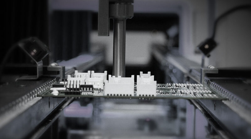
Jeśli chodzi o świat projektowania i produkcji PCB, Płytki obwodów drukowanych play a pivotal role in testing and validation processes. Whether you’re an engineer, a designer, or simply someone interested in electronics, understanding the nuances of Płytki obwodów drukowanych is essential for ensuring product performance and reliability. In this article, we’ll delve into what load board PCBs are, their applications, benefits, and best practices in their design and usage.
Co to jest płytka obwodu drukowanego?
A load board PCB, often referred to as a test board, is specifically designed to facilitate electrical testing. It serves as a physical interface between the device under test (DUT) and the test equipment. The primary function of a load board is to apply electrical loads to the DUT, allowing engineers to perform essential tests such as functionality, performance validation, and signal integrity analysis.
The Importance of Load Board PCBs in Testing
Load board PCBs are crucial in the testing phase of electronic devices for several reasons:
- Wydajność: Load boards streamline the testing process by providing a standardized interface that reduces setup time and complexity.
- Dokładność: With precise load conditions, testing results are more reliable, allowing for better detection of potential defects.
- Efektywność kosztowa: Investing in load boards can decrease overall testing costs by reducing the need for excessive prototypes and tests.
Applications of Load Board PCBs
Load board PCBs find applications across various industries:
- Elektronika użytkowa: Testing smartphones, tablets, and personal gadgets.
- Motoryzacja: Ensuring the reliability of electronic components in vehicles.
- Telekomunikacja: Validating signal integrity in communication devices.
- Przemysł lotniczy i obronny: Rigorous testing of critical systems and components.
Key Components of Load Board PCBs
Understanding the structure of load board PCBs is crucial for effective design and usage. Here are some key components typically found in load board PCBs:
- Test Probes: These are used to make contact with the DUT, allowing for measurements and diagnostics.
- Rezystory i kondensatory: These components create specific load conditions for the DUT.
- Connectors: Standardized connectors ensure compatibility with various DUTs and test equipment.
- Samoloty naziemne: Providing a stable reference for electrical testing, which improves signal integrity.
Design Considerations for Load Board PCBs
Designing an effective load board PCB requires attention to several factors:
- Layout: The PCB layout must minimize interference and maintain proper ground connections to ensure accurate testing results.
- Integralność sygnału: High-speed signals require careful consideration of trace lengths and types to avoid signal degradation.
- Zarządzanie temperaturą: Adequate heat dissipation is vital, especially for high-power applications, to prevent damage during testing.
- Elastyczność: Designing load boards that can accommodate multiple DUTs can save time and resources.
Best Practices for Using Load Board PCBs
To maximize the effectiveness of load board PCBs, consider the following best practices:
- Dokładne procedury testowe: Establish standardized testing protocols to ensure consistent outcomes.
- Regularna konserwacja: Periodically inspect and maintain load boards to ensure they remain in optimal condition.
- Dokumentacja: Keep detailed records of test results, configuration settings, and modifications to provide context for future tests.
- Personel pociągu: Ensure that all personnel involved in testing are adequately trained to handle the load boards and associated equipment.
Future Trends in Load Board PCB Technology
The field of PCB testing is continuously evolving, and several trends are emerging in load board technology:
- Automatyzacja: Increasing automation in testing will enhance efficiency and accuracy.
- Integracja: There is a growing trend towards integrating multiple test functionalities into single load boards, reducing the need for multiple devices.
- Miniaturyzacja: As electronic devices become smaller, load boards will need to adapt to fit new form factors while maintaining testing efficacy.
- Inteligentne technologie: Leveraging IoT and AI technologies for predictive maintenance and automated testing processes.
Conclusion: Driving Quality through Load Board PCBs
In the fast-paced world of electronics, load board PCBs are indispensable for maintaining quality and reliability in testing processes. Their ability to simulate real-world conditions allows engineers to ensure that their products meet the highest standards before they reach the market. Understanding load board PCBs’ design and application will empower professionals to harness their full potential and drive innovation in electronic testing.


