Power electronics have revolutionized the way we harness and use energy, and one of the cornerstones of this innovation is the inverter. Central to any inverter’s functionality is its Printed Circuit Board (PCB) assembly, which is essential for the conversion of DC power into AC power. In this article, we will explore the PCB assembly process for inverters, its significance, various components involved, manufacturing techniques, and quality assurance practices.
What is an Inverter?
An inverter is an electronic device that converts direct current (DC) into alternating current (AC). This capability is crucial for various applications, including solar energy systems, electric vehicles, uninterruptible power supplies (UPS), and various household appliances. While the concept seems straightforward, the complexity arises in the internal workings of inverters, primarily within the realm of PCB assembly.
The Role of PCB in Inverter Functionality
The PCB serves as the backbone of the inverter system, providing a platform for interconnecting electronic components. It integrates various elements such as capacitors, inductors, diodes, and transistors, each playing a specific role in the functioning of the inverter. The layout, design, and assembly of these components on the PCB are pivotal for achieving optimal performance and reliability.
Components of PCB Assembly in Inverters
1. **Microcontroller or Microprocessor**: Acts as the brain of the inverter, controlling the entire operation and ensuring that the output AC waveform matches the required specifications.
2. **Power Semiconductors**: These include MOSFETs or IGBTs, responsible for switching the current and controlling the power output of the inverter.
3. **Passive Components**: Resistors, capacitors, and inductors that help in filtering, smoothing, and conditioning the voltage and current levels within the circuit.
4. **Cooling Solutions**: Given that inverters generate heat during operation, effective thermal management components such as heat sinks or fans are essential to prolong the lifespan of the device.
PCB Design Considerations for Inverters
The design of the PCB is critical to the efficiency and performance of the inverter. Several factors must be taken into account:
- Trace Width and Thickness: The width and thickness of the traces on the PCB must be designed to handle the expected current load without excessive heat generation.
- Component Placement: Optimal placement reduces electromagnetic interference (EMI) and improves the overall performance by minimizing the length of connections between components.
- Thermisch beheer: Adequate space must be allocated for components that generate heat, with consideration for airflow and thermal dissipation.
- Ground Planes: Implementing solid ground planes can significantly improve the electrical performance and reliability of the power circuits.
Technieken voor PCB-assemblage
The assembly of PCBs in inverter technology can be performed using various methods, primarily divided into two categories: through-hole and surface mount technology (SMT).
Through-Hole Technology
This older method requires components to be inserted into pre-drilled holes on the PCB and soldered on the opposite side. While it can be easier to repair, it is less commonly used in modern inverter applications due to the increased demand for compactness and efficiency.
SMT (Surface Mount Technology)
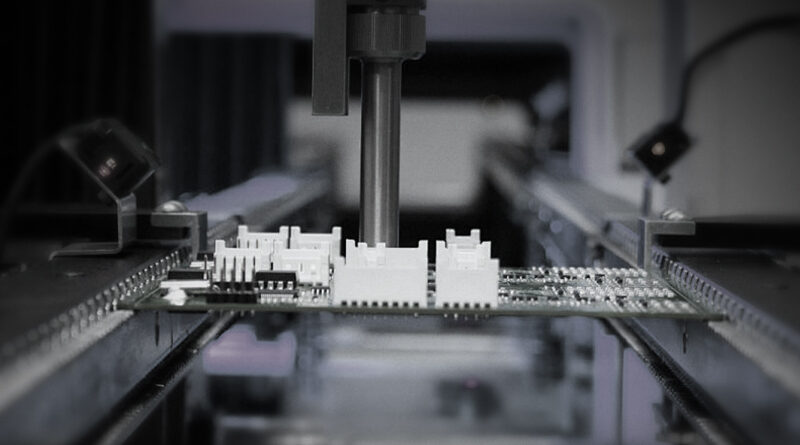
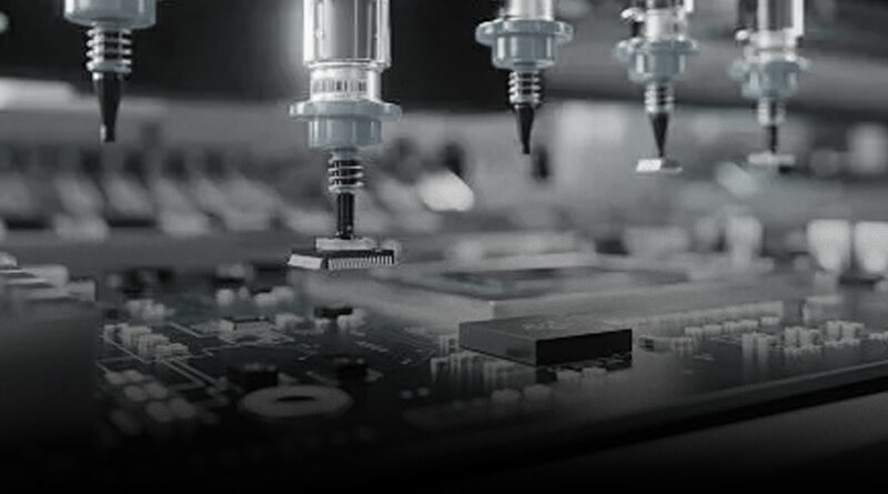
SMT has become the standard for PCB assembly in inverter technology. It allows for components to be mounted directly onto the surface of the PCB, enabling higher component density and improved performance. SMT also benefits from automated assembly processes, contributing to cost-efficiency and production scalability.
Kwaliteitsborging in PCB-assemblage
Ensuring the reliability and authenticity of the PCB assembly is paramount in inverter technology, as any failure can lead to significant operational issues. Effective quality assurance practices include:
- Visual Inspection: Inspecting the PCB for defects in soldering, component placement, and overall layout.
- Geautomatiseerde optische inspectie (AOI): Using specialized machines to verify the assembly process electronically, ensuring no defects go unnoticed.
- Functioneel testen: Testing the completed inverter circuit under operational conditions to ensure it meets specified performance criteria.
- Reliability Testing: Conducting stress tests and thermal cycling to analyze the long-term performance of the assembled PCB.
Toekomstige trends in PCB-assemblage van omvormers
As technology progresses, the PCB assembly for inverters is expected to evolve, influenced by advancements in materials, component technology, and manufacturing processes. Trends to watch out for include:
- Higher Integration: With the rise of System-on-Chip (SoC) technologies, more functionalities will be integrated into a single chip, reducing PCB size and complexity.
- Flexible PCBs: The utilization of flexible PCB materials could revolutionize housing designs in inverters, allowing for more innovative layouts and applications.
- Enhanced Thermal Management: Ongoing research will likely yield new materials and designs for improved thermal dissipation, ensuring longer life cycles for inverters.
- Smart Inverters: As smart technologies become prevalent, inverters will incorporate IoT capabilities, making connectivity and real-time monitoring a standard feature.
Conclusie
In summary, the role of PCB assembly in inverter technology cannot be overstated. As the demand for efficient and reliable power conversion continues to grow, mastering the intricacies of PCB design, assembly, and testing will be essential for industry professionals. This evolving field is rife with opportunities for innovation, pushing the boundaries of what inverters can achieve in our increasingly electronic landscape.


