As the electronics industry continues to advance rapidly, the need for reliable and sophisticated methods of quality assurance becomes ever more crucial. One of the most effective technologies in this regard is X-ray imaging for Printed Circuit Boards (PCBs). This method not only enhances quality control but also significantly reduces production costs and risks associated with faulty electronics. Whether you’re a manufacturer, quality manager, or an enthusiast, understanding the basics and benefits of PCB board X-ray technology is essential in staying ahead in this competitive field.
What is PCB Board X-Ray Technology?
PCB board X-ray technology involves the use of high-energy radiation to visualize the internal structures of a printed circuit board. This non-destructive testing method enables the detection of defects and anomalies within a PCB assembly that are not visible to the naked eye. From solder joint integrity to component placement, X-ray inspection provides invaluable insight that can significantly improve the manufacturing process.
The Science Behind PCB X-Ray Imaging
X-rays are a form of electromagnetic radiation that can penetrate various materials, including metals and plastics that commonly comprise circuit boards. When an X-ray beam passes through a PCB, different materials absorb the rays at different rates. This differential absorption creates contrast on the resulting X-ray image, allowing operators to identify defects.
Modern X-ray systems for PCB inspection typically utilize digital imaging technology. This results in high-resolution images that can be analyzed for irregularities such as:
- Leemtes in soldeerverbindingen
- Verkeerde uitlijning van onderdelen
- Buried vias
- Cracks or fractures in components
Why Use PCB X-Ray Technology?
Implementing X-ray inspection in PCB manufacturing presents numerous advantages:
1. Niet-destructief onderzoek
One of the greatest benefits of X-ray technology is its non-destructive nature. Unlike other testing methods that may compromise the integrity of the PCB, X-ray images can be obtained without affecting the actual product, allowing for ongoing quality assurance throughout the manufacturing process.
2. Verbeterde detectie van verborgen defecten
Many defects are concealed within multiple layers of solder and components. X-ray technology helps to pinpoint these hidden issues effectively, ensuring that manufacturers can address potential problems before they escalate and lead to product failures.
3. Snelheid en efficiëntie
In a fast-paced production environment, efficiency is key. X-ray inspection can process PCBs quickly, facilitating immediate feedback that maximizes productivity. With reduced downtime, manufacturers can achieve tighter deadlines without compromising on quality.
4. Kosteneffectiviteit
While the initial investment in X-ray technology may be significant, the long-term savings can be considerable. By catching defects early in the manufacturing process, companies can reduce rework costs, minimize returns, and improve overall customer satisfaction.
How PCB X-Ray Inspection Works
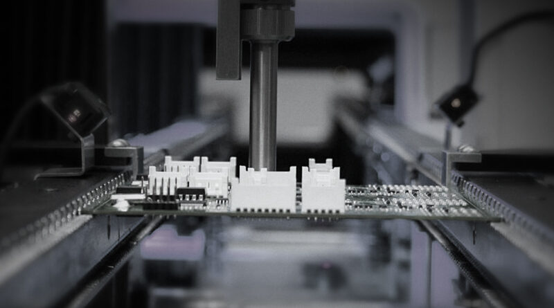
The PCB X-ray inspection process begins with the placement of the board on a conveyor system that moves into the X-ray machine. Once in place, the X-ray source emits rays that penetrate the board, generating images captured by digital detectors. These images are then stored and can be displayed on monitors for detailed analysis.
What to Look for in an X-Ray Inspection System
When selecting an X-ray inspection system for PCB testing, several factors should be considered:
- Beeldkwaliteit: Look for systems providing high-resolution images necessary for identifying minute defects.
- Software mogelijkheden: Advanced software should enable automated inspections, reporting features, and user-friendly interfaces.
- Doorvoer: Ensure the system can handle your production volume without sacrificing speed.
- Ondersteuning en service: Partner with a supplier that offers robust technical support and maintenance services.
Common Applications for PCB X-Ray Technology
PCB X-ray technology is a versatile tool applicable across various sectors, including:
1. Consumentenelektronica
The consumer electronics sector has seen a tremendous increase in complexity. X-ray inspection helps ensure the reliability of devices such as smartphones, tablets, and wearables by detecting defects at early stages.
2. Medische hulpmiddelen
In the medical field, the safety of devices is paramount. X-ray technology provides verification of the assembly integrity of life-saving equipment.
3. Aerospace and Automotive
In high-stakes industries like aerospace and automotive, X-ray inspection helps maintain performance and safety standards by ensuring that critical systems function reliably.
Beste werkwijzen voor PCB-röntgeninspectie
For optimal results from your PCB X-ray inspections, consider the following practices:
- Regelmatige kalibratie: Ensure the X-ray system is calibrated regularly to maintain accuracy and reliability.
- Operatortraining: Invest in comprehensive training for operators to maximize the capability of the X-ray system.
- Gegevensbeheer: Implement a robust data management system to track inspection results and identify trends over time.
Future of X-Ray Technology in PCB Inspection
As technology evolves, we can expect even more sophisticated advancements in X-ray technology for PCB inspection. Innovations such as 3D imaging and artificial intelligence applications are on the horizon, promising to enhance defect detection capabilities and streamline inspection processes further.
Ultimately, as the demand for higher quality electronics continues to grow, PCB board X-ray technology will play an increasingly vital role in ensuring manufacturing excellence. By investing in this powerful inspection method, manufacturers can maintain high standards and secure their place in an ever-evolving market.


