In the fast-paced world of electronics and PCB (Printed Circuit Board) manufacturing, quality assurance is paramount. As devices become smaller and more complex, traditional inspection methods often fall short. This article dives into the critical role of X-ray inspection technology in enhancing the quality and reliability of PCBs—a method that is transforming the landscape of electronics manufacturing.
PCB 제조의 이해
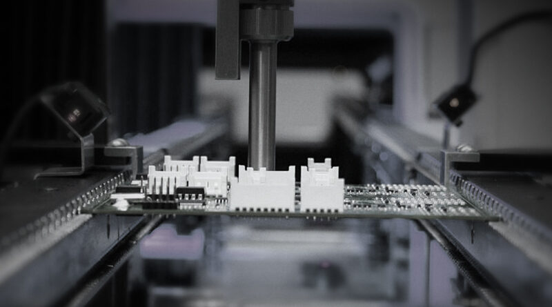
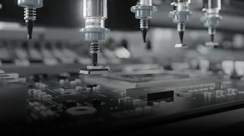
PCBs are the backbone of modern electronic devices, providing the necessary circuitry to connect various components. The manufacturing process involves several critical steps, including design, etching, soldering, and assembly. Each step must meet stringent quality standards to ensure the functionality and longevity of the final product.
Why Inspection is Important
Any defects in a PCB can lead to catastrophic failures in electronic devices. Common issues such as cold solder joints, voids, misalignments, and other defects can significantly impact performance. Therefore, robust inspection processes are essential to identify and rectify issues early in the manufacturing cycle.
Introduction to X-Ray Inspection Technology
X-ray inspection is a non-destructive testing method that uses X-rays to examine the internal structures of PCBs without causing any damage. This technology allows manufacturers to visualize hidden features and verify component placement and solder joint integrity, providing invaluable insights that are critical for high-quality production.
엑스레이 검사의 이점
- 비파괴 검사: Unlike other testing methods, X-ray inspection does not damage the boards, allowing for full analysis before final assembly.
- 높은 정확도: X-ray systems can detect minute defects that may be invisible to the naked eye or traditional inspection methods.
- 효율성: Automated X-ray inspection (AXI) systems process boards quickly, allowing for high throughput in manufacturing environments.
- 종합 분석: X-ray can identify issues such as hidden voids in solder joints, which are not detectable through external inspections.
- 실시간 피드백: Manufacturers can receive immediate feedback on production quality, enabling faster adjustments and reducing waste.
X-Ray Inspection Techniques
1. 2D 엑스레이 검사
Two-dimensional X-ray inspection provides a flat image of the PCB, allowing operators to inspect critical areas, such as solder joints and component placements. This method is efficient for detecting major issues but may not provide sufficient detail for complex assemblies.
2. 3D 엑스레이 검사
Three-dimensional X-ray inspection provides a volumetric analysis of the PCB. This advanced method offers a detailed view of the internal structures, making it easier to identify hidden defects, such as air pockets within solder joints or misalignments.
3. Computed Tomography (CT)
Computed tomography (CT) is the most sophisticated form of X-ray inspection. It takes multiple X-ray images from various angles and reconstructs them into a 3D model of the PCB. This technique provides the most comprehensive analysis and is particularly valuable for complex multilayer boards.
Application of X-Ray Inspection in Different Industries
X-ray inspection is not limited to standard consumer electronics. Its applications extend across various industries, including:
- 의료 기기: Ensuring the reliability of medical devices where failures could lead to serious consequences.
- 항공우주: Critical components in aerospace applications require the highest quality standards due to safety implications.
- 자동차: As cars become more reliant on electronic systems, robust inspection methods are essential for component reliability.
- 통신: High-quality PCB components are vital in maintaining communication systems’ integrity.
도전 과제 및 고려 사항
Despite its numerous advantages, implementing X-ray inspection systems can pose challenges. The high initial investment for advanced systems may be prohibitive for some manufacturers. Moreover, X-ray inspection requires skilled personnel to operate the equipment and interpret the results accurately.
Additionally, manufacturers must consider the size and complexity of the PCBs they are inspecting. Not all X-ray systems are designed to handle large or densely populated boards, necessitating a careful selection process when integrating this technology into manufacturing workflows.
PCB 제조에서 X-Ray 검사의 미래
As technology continues to advance and the demand for high-quality, reliable PCBs increases, the role of X-ray inspection in PCB manufacturing will only grow. Companies are investing in research and development to improve X-ray technologies, making them more efficient, faster, and accessible.
The rise of automation and integration with artificial intelligence will also enhance the capabilities of X-ray inspection systems, allowing for intelligent defect detection and predictive maintenance strategies that further enhance the reliability of PCBs.
엑스레이 검사 구현을 위한 모범 사례
For manufacturers considering implementing X-ray inspection, following best practices is crucial for maximizing the benefit of this technology:
- Evaluate Needs: Assess specific inspection requirements and ensure that the selected system aligns with production goals.
- Train Personnel: Invest in training for operators to ensure accurate use and interpretation of X-ray data.
- 정기 유지 관리: Schedule regular maintenance and calibration of X-ray systems to ensure consistent performance.
- Integrate with Other QA Processes: Combine X-ray inspection with other quality assurance methods for a comprehensive approach to manufacturing quality.
In conclusion, as PCB manufacturing continues to evolve, X-ray inspection represents a significant step forward in ensuring the quality and reliability of electronic devices. With its ability to provide detailed insights into the internal structures of PCBs, X-ray technology is set to play an even more pivotal role in the future of electronics manufacturing.


