El mundo de la fabricación electrónica es rico en complejidad e innovación. A medida que se dispara la demanda de dispositivos electrónicos sofisticados, es crucial comprender los procesos clave, como la soldadura por reflujo SMT, la inspección óptica automatizada (AOI), la inspección por rayos X y el grabado por láser. En esta entrada de blog, profundizaremos en cinco experiencias notables que ilustran la importancia y los entresijos de estas tecnologías en el montaje moderno de placas de circuito impreso.
1. Dominio del proceso de reflujo SMT
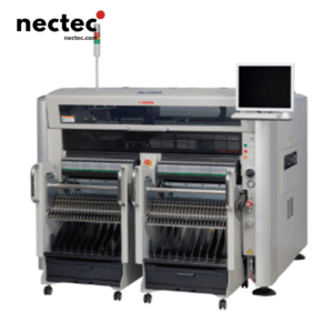
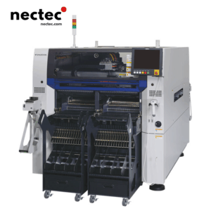
Una de mis primeras experiencias en el ámbito de la fabricación electrónica fue en unas instalaciones dedicadas a la producción de tecnología de montaje superficial (SMT). Aprendí rápidamente que el proceso de reflujo no consiste sólo en fundir soldadura para conectar componentes. Se trata de un calentamiento de precisión, en el que la placa de circuito impreso pasa por un horno de reflujo con un perfil de temperatura cuidadosamente controlado. La clave de este proceso es comprender que los distintos componentes requieren temperaturas diferentes, lo que plantea el reto de garantizar que las piezas sensibles no resulten dañadas.
Esto quedó patente cuando trabajamos en un prototipo que debía soportar un gran estrés térmico. El proceso de reflujo tenía que calibrarse meticulosamente para evitar choques térmicos y garantizar al mismo tiempo que la soldadura mojara adecuadamente las almohadillas. Descubrí que el uso de equipos de perfilado térmico mejoraba significativamente nuestros resultados, ya que nos permitía visualizar y ajustar dinámicamente el ciclo de calentamiento. Esta experiencia me enseñó la importancia de invertir en la tecnología y los conocimientos adecuados para perfeccionar el proceso de reflujo, demostrando lo vital que es para la calidad general del montaje de placas de circuito impreso.
2. Implantación de sistemas AOI
Tras perfeccionar mis habilidades en el reflujo SMT, pasé a centrarme en el proceso de inspección óptica automatizada (AOI). Durante un proyecto en el que aumentamos la producción para un cliente de gran volumen, los sistemas AOI ayudaron a mantener el control de calidad a niveles sin precedentes. La velocidad de estas máquinas es asombrosa, ya que pueden escanear las placas de circuito impreso en busca de defectos en tiempo real, analizando la posición de cada componente, la calidad de las juntas de soldadura e incluso la presencia de piezas que faltan.
Sin embargo, me di cuenta de que no todos los diseños de placas de circuito impreso eran iguales; algunos requerían perfiles de AOI personalizados que tuvieran en cuenta las formas o disposiciones únicas de los componentes. Además, era crucial formar al personal para que comprendiera los resultados y tomara decisiones fundamentadas basándose en los datos de AOI. Una experiencia que destaca es cuando detectamos un componente desalineado en una placa de circuito impreso destinada a dispositivos médicos. Gracias al sistema AOI, pudimos detener la producción, identificar la causa y aplicar medidas correctivas antes de que ningún dispositivo defectuoso saliera de la línea de montaje. Esta experiencia puso de manifiesto la importancia de la AOI no sólo para mantener la calidad, sino también para garantizar la seguridad de los dispositivos electrónicos.
3. El papel de la inspección por rayos X
A medida que los ensamblajes de placas de circuito impreso se hacían más complejos, también aumentaba nuestra dependencia de técnicas de inspección avanzadas. Esto me llevó a conocer la inspección por rayos X mientras trabajaba en un proyecto de ensamblaje de BGA ciegos. A primera vista, las ventajas de la inspección por rayos X son evidentes: nos permite mirar bajo la superficie y evaluar conexiones que de otro modo quedarían ocultas. Recuerdo vívidamente la primera vez que observé un análisis con rayos X de un componente BGA. La posibilidad de visualizar las juntas de soldadura en busca de huecos o defectos supuso un cambio radical.
Además, la inspección por rayos X reveló que el perfil de reflujo que habíamos estado utilizando no eliminaba sistemáticamente los huecos en las juntas de soldadura, lo que podía provocar problemas de rendimiento. Al identificar áreas problemáticas concretas, pudimos perfeccionar nuestros procesos y, en última instancia, mejorar la fiabilidad de nuestro producto final. Esta experiencia puso de relieve la importancia de integrar múltiples métodos de inspección para lograr un conocimiento exhaustivo de la calidad de nuestra producción.
4. Exploración de las innovaciones del grabado por láser
Otra área apasionante que tuve el privilegio de explorar fue el grabado láser. Con la tendencia a la miniaturización de la electrónica, observamos una creciente demanda de marcas precisas y de alta calidad en las placas de circuito impreso. Mi equipo empezó a aplicar el grabado láser no sólo para marcar, sino como parte esencial del seguimiento y la gestión de calidad. El grabado láser me impresionó porque utiliza luz focalizada para crear marcas precisas y permanentes que pueden soportar los rigores del entorno de producción.
Un proyecto memorable consistió en grabar códigos QR en placas de circuito impreso con fines de trazabilidad. Estos códigos nos permitieron rastrear fácilmente los componentes a lo largo de la cadena de suministro, mejorando nuestra capacidad para gestionar el inventario y las reclamaciones de garantía. La versatilidad del grabado láser, desde la fabricación de prototipos hasta la producción de grandes tiradas, demostró ser inestimable. Se hizo evidente que invertir en tecnología láser no era una mera tendencia, sino una decisión estratégica a largo plazo que encajaba bien con nuestros objetivos de mejorar la calidad y la eficiencia.
5. Integración de procesos para una mayor eficiencia
Por último, mis experiencias en reflujo SMT, AOI, rayos X y grabado láser culminaron en una importante iniciativa de optimización de procesos dentro de la línea de montaje. Conscientes de que cada paso de inspección y fabricación influye en los demás, intentamos minimizar los cuellos de botella y mejorar el flujo de materiales. Un ejemplo de ello fue nuestro enfoque para integrar más estrechamente la inspección AOI y por rayos X en nuestro proceso de reflujo. Al coordinar estas inspecciones, redujimos significativamente los tiempos de espera y mejoramos nuestra eficiencia general.
Este viaje me enseñó que la colaboración y la comunicación entre departamentos son vitales para agilizar los procesos. Durante la producción, la celebración de reuniones periódicas nos permitió compartir ideas y ajustar nuestro enfoque en función de los datos en tiempo real. La integración de tecnologías como AOI y rayos X en nuestro flujo de trabajo no sólo redujo los tiempos de ciclo, sino que también reforzó nuestros esfuerzos de control de calidad. En última instancia, esta experiencia reforzó la idea de que la interacción de estas tecnologías es lo que impulsa la innovación en el sector de la fabricación de productos electrónicos, lo que nos permite satisfacer las demandas en constante evolución de los consumidores.
Reflexiones finales
Cuando reflexiono sobre estas cinco experiencias fundamentales -el dominio del reflujo SMT, la implantación de sistemas AOI, el papel fundamental de la inspección por rayos X, la exploración de las innovaciones del grabado láser y la integración de procesos-, queda claro que cada tecnología desempeña un papel único, aunque interconectado, en el panorama de la fabricación de productos electrónicos. Para tener éxito, hay que adaptarse continuamente, aprender y adoptar la innovación. Sólo comprendiendo estos diversos procesos podremos garantizar la máxima calidad en la producción de dispositivos electrónicos.