Printed Circuit Boards (PCBs) are the backbone of modern electronics, facilitating the connection and operation of various components. As technology advances, the demand for more intricate designs continues to rise, leading to an increased focus on the loading process of PCBs. In this guide, we’ll delve into the various techniques of Zatížení desek plošných spojů, potential challenges faced during the process, and effective solutions to ensure optimal performance and reliability.
Porozumění zatížení desek plošných spojů
Zatížení desek plošných spojů refers to the process of placing electronic components onto a printed circuit board’s surface. This process can significantly affect the performance and functionality of the final product. It involves several factors, such as the type of components used, their orientation, and the overall layout of the PCB. Proper loading is critical for maintaining signal integrity, reducing electromagnetic interference (EMI), and ensuring efficient thermal management within the device.
Typy technik vkládání desek plošných spojů
Several loading techniques are commonly employed in PCB assembly. The choice of technique often depends on the specific requirements of the electronic device and the manufacturing capabilities of the assembly house. Here’s a closer look at the most popular PCB loading methods:
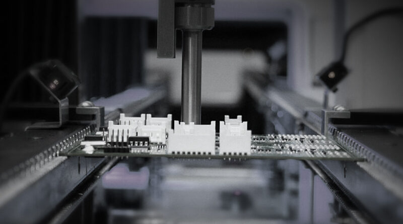
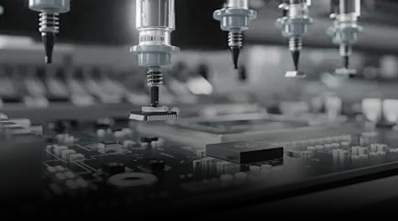
- Technologie povrchové montáže (SMT): This method places components directly onto the surface of the PCB. SMT components are smaller, allowing for higher density and more compact designs. The process requires precise soldering techniques and often employs automated pick-and-place machines for efficiency.
- Through-Hole Technology (THT): In THT, components are inserted through holes in the PCB and soldered on the opposite side. This method is typically used for larger components or in applications requiring enhanced mechanical stability.
- Smíšené technologie: Combining both SMT and THT allows engineers to leverage the benefits of each approach. This technique is advantageous when different components with varying physical dimensions and electrical requirements are used.
Challenges in PCB Loading
Despite advancements in technology, numerous challenges continue to plague the PCB loading process. Understanding these hurdles is essential for achieving optimal outcomes. Here are some common challenges:
1. Přesnost umístění komponent
Precise component placement is crucial for multitasking PCBs. Even minimal inaccuracies can lead to misaligned pins, resulting in weak connections and potential device failure. Maintaining high tolerances in placement using automated systems can be expensive but is necessary for high-performance applications.
2. Tepelné řízení
Heat dissipation is a significant concern in densely packed PCBs. Components that generate excessive heat can damage sensitive parts, leading to unreliable operation. Engineers must consider the thermal profile of the board and implement proper heat dissipation techniques, such as adding cooling pads or using heat sinks.
3. Signal Integrity
As operating frequencies increase, ensuring signal integrity becomes challenging. High-frequency signals are susceptible to crosstalk and EMI, which can distort the signals transmitted across the PCB. Designing for controlled impedance is essential to mitigate these effects.
Solutions for Effective PCB Loading
To tackle the challenges associated with PCB loading, several strategies can be employed:
1. Advanced Simulation Tools
Utilizing simulation software can help engineers visualize the PCB design and assess the effects of various loading techniques before production. These tools allow for the analysis of thermal dynamics, signal integrity, and mechanical stability, reducing the likelihood of errors during manufacturing.
2. Implementing Design for Manufacturability (DFM) Principles
Incorporating DFM principles during the design phase can significantly improve the ease of assembly and overall performance of PCBs. This approach emphasizes simplicity and reliability in the component loading process.
3. Regular Quality Control Inspections
Maintaining stringent quality control measures throughout the PCB manufacturing process ensures that potential issues are caught early. Conducting regular inspections, such as Automated Optical Inspection (AOI) and X-ray analysis for solder joints, helps maintain high standards of accuracy and reliability.
The Future of PCB Loading
As the electronics industry constantly evolves, so too will the PCB loading techniques. Innovations in materials and manufacturing processes will lead to more compact, efficient, and reliable designs. Technologies like 3D printing and advanced robotics are beginning to play a critical role in PCB assembly, enabling the development of complex geometries and customized solutions.
Moreover, the increasing demand for wearable technology, IoT devices, and automotive applications presents new challenges and opportunities for PCB loading processes. Engineers must stay abreast of the latest trends and adapt their designs accordingly to meet the ever-changing landscape of technology.
Závěrečné myšlenky
Given the vital role that PCB loading plays in electronic device performance, understanding the techniques, challenges, and solutions is crucial for professionals in the industry. As manufacturers continue to innovate and develop more advanced processes, the standards for PCB loading will evolve, emphasizing the importance of quality, precision, and efficiency.


